








Most LED failures reach the customer as a system symptom: a dead pixel in a display, a security camera that goes blind at night, a curing module that stops initiating adhesive, or an indicator that reads the wrong state on a machine panel. Reliability engineering begins by reversing that translation, tracing the symptom back to the mechanism that caused it, and then back to the package and process decision that allowed the mechanism to act. This atlas is a cross-reference between package families and the failure mechanisms that dominate them, with the field signature and the single most decisive diagnostic test for each.
1. Why failure mechanisms correlate with package type
An LED package is a set of material interfaces: die to submount, submount to lead frame or ceramic, encapsulant to package wall, wire bond to pad, solder joint to MCPCB. Each interface has a different coefficient of thermal expansion, a different permeability to moisture and sulfur, and a different tolerance for mechanical stress. Because package families differ in which interfaces they contain and how they are constructed, they differ in which mechanism fails first under a given environmental stress.
Three design axes explain most of the variation. Encapsulation chemistry determines resistance to sulfur and ultraviolet discoloration. Die attach material (silver epoxy versus gold-tin eutectic versus sintered silver) sets the thermal path and the maximum junction temperature. Body material (PPA, PCT, EMC, or ceramic) governs moisture permeation and reflow tolerance. Mapping a field failure to a package family therefore narrows the candidate mechanisms before any laboratory work begins.
| Package family | Encapsulation | Die attach | Body | Dominant risk |
|---|---|---|---|---|
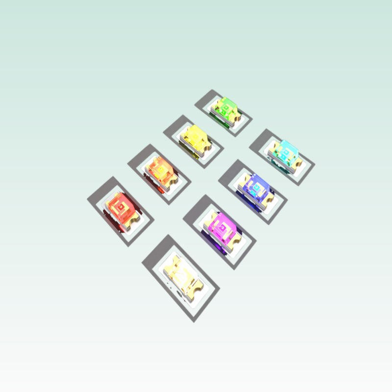
| 2835 / 3528 SMD | Silicone or epoxy | Silver epoxy | PPA / PCT | Sulfurization, lumen decay |
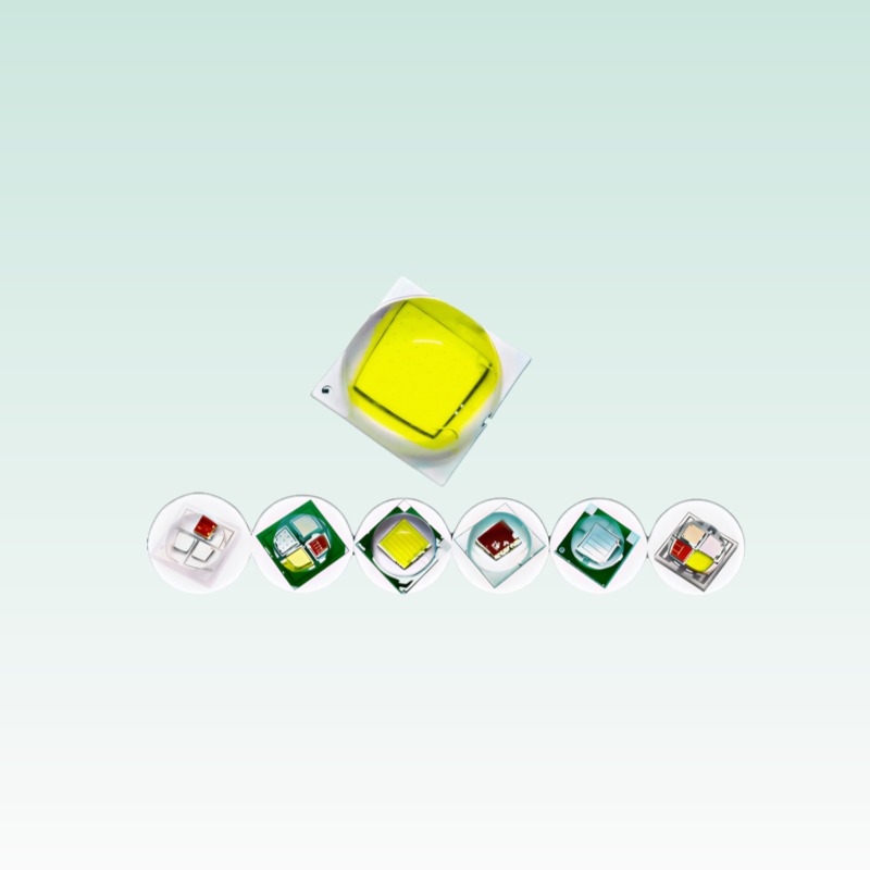
| 3535 / 5050 ceramic | Silicone + glass | Eutectic AuSn | AlN ceramic | Delamination, CTE fatigue |
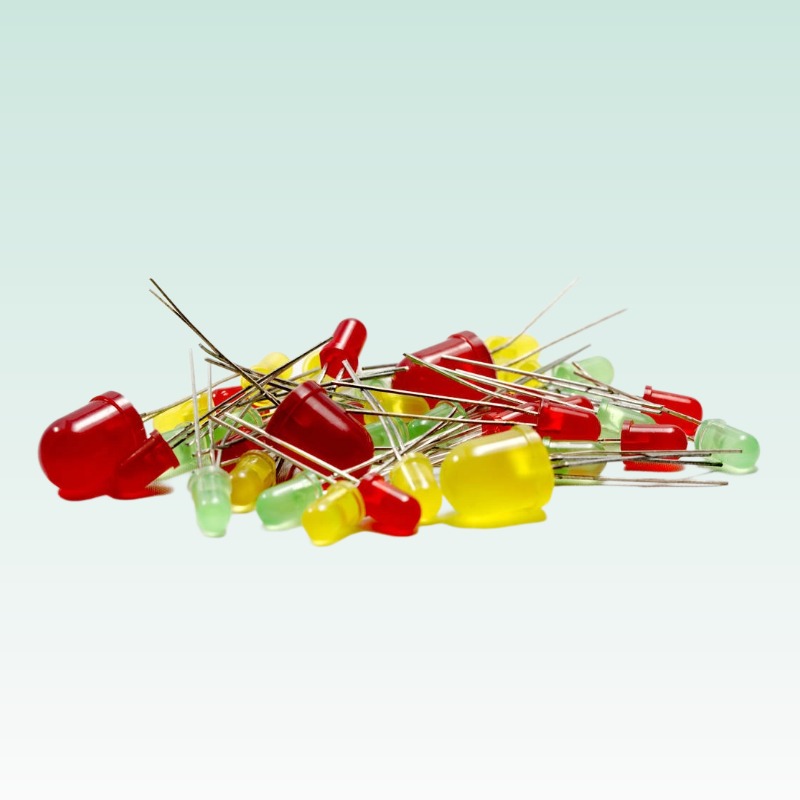
| 5 mm DIP | Epoxy lens | Silver epoxy | Epoxy lens | Lens yellowing, wire fatigue |
| COB array | Silicone dome | Sintered silver or epoxy | Aluminium / ceramic | Phosphor thermal quenching |
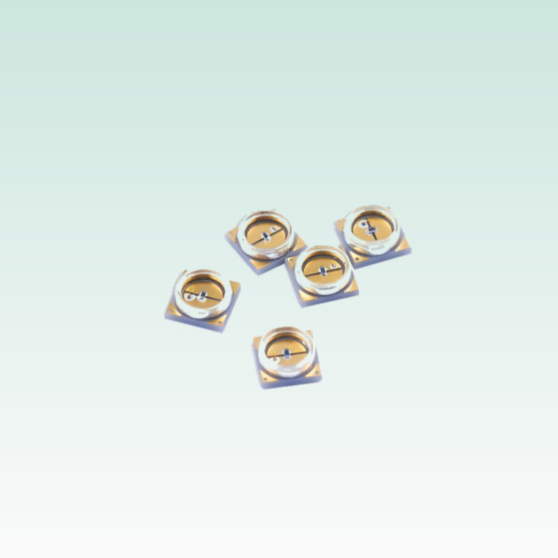
| UV ceramic | Quartz or hard glass | Eutectic AuSn | AlN ceramic | Seal degradation, encapsulant UV haze |
2. The failure mode / package cross-reference atlas
The grid below is the core of this atlas. Read across a row to see which packages are vulnerable to a mechanism; read down a column to see which mechanisms threaten a package.
| Failure mechanism | SMD plastic | Ceramic HP | DIP | COB | UV ceramic | Field signature |
|---|---|---|---|---|---|---|
| Sulfurization (Ag corrosion) | High | Low | Medium | Low | Low | Gradual dimming, dark pad, low flux |
| Delamination (die / encapsulant) | Medium | High | Low | Medium | High | Sudden drop, optical artifacts |
| Wire bond fatigue | Medium | Low | High | Low | Low | Intermittent, opens when hot |
| ESD / EOS damage | High | Medium | High | Medium | Medium | Immediate dead or leaky die |
| Phosphor thermal quenching | Low | Medium | Low | High | n/a | Colour shift with current |
| Encapsulant UV haze | Medium | Medium | Medium | Medium | High | Slow output loss, yellowing |
| Solder joint cracking | High | Medium | Low | High | Medium | Opens after thermal cycling |
| Lens yellowing (epoxy) | Medium | Low | High | Low | Low | Gradual CCT shift + dimming |
3. Mechanism reference: activation energy and test correlation
Each mechanism accelerates with temperature according to an Arrhenius relationship, and with humidity or bias according to its own physics. The table gives the activation energy used for lifetime extrapolation and the accelerated test that most directly reproduces the mechanism.
| Mechanism | Activation energy Ea (eV) | Accelerated test | Test standard | Typical acceleration |
|---|---|---|---|---|
| Sulfurization | 0.50–0.70 | Sulfur vapour, 60 °C / high RH | IEC 60068-2-43 (H2S) | 5–15× |
| Encapsulant UV haze | 0.30–0.45 | UV preconditioning, 85 °C | IEC 60068-2-5 | 10–20× |
| Die / encapsulant delamination | 0.35–0.55 | Thermal shock -40 to 125 °C | JESD22-A104 | 20–50× |
| Wire bond fatigue | 0.60–0.80 | Power cycling ΔT 60–100 K | JESD22-A105 | 15–30× |
| Solder joint cracking | 0.70–0.90 | Thermal cycling 0 to 100 °C | JESD22-A104 | 10–25× |
| ESD / EOS | n/a (not Arrhenius) | HBM / MM / CDM discharge | ANSI/ESDA/JEDEC JS-001 | pass/fail |
| Phosphor thermal quenching | n/a (reversible) | Current step, Tj sweep | In-house | pass/fail |
The acceleration factor follows the Arrhenius equation:
AF = exp[ (Ea / k) × (1/T_use - 1/T_stress) ]
where k is the Boltzmann constant (8.617 × 10⁻⁵ eV/K) and temperatures are in kelvin. A mechanism with Ea = 0.7 eV tested at 125 °C against a 55 °C use condition yields AF ≈ 47, meaning 100 hours of stress represents roughly 4,700 hours of field life for that mechanism alone.
4. Diagnostic flow: from symptom to confirmed mechanism
Failure analysis proceeds by narrowing, not by guessing. The four stages below should be worked in order, because each stage is cheaper than the next and each one eliminates candidates.
- Electrical screening. Measure forward voltage at rated current and reverse leakage at rated reverse voltage. A shift in Vf of more than 0.2 V, or reverse leakage above the datasheet limit, indicates die-level or bond-level damage and points toward ESD/EOS or wire fatigue rather than a gradual material degradation.
- Optical characterization. Measure flux and peak wavelength at fixed current and fixed case temperature. A flux loss with stable wavelength suggests encapsulant or phosphor degradation; a wavelength shift suggests junction temperature change or phosphor damage.
- Non-destructive physical inspection. X-ray radiography reveals wire bond geometry and solder voiding. Scanning acoustic microscopy (C-SAM) maps delamination at the die attach and encapsulant interfaces. Neither step damages the sample.
- Destructive physical analysis. Selective de-processing (laser decapsulation or chemical etch), then SEM and EDS of the die surface and bond pads. EDS identifies sulfur, chlorine or oxygen compounds and confirms or refutes the mechanism hypothesis from stages 1–3.
| Stage | Method | Confirms | Sample survives |
|---|---|---|---|
| 1 | I-V curve trace | ESD/EOS, wire fatigue | Yes |
| 2 | Integrating sphere, spectroradiometer | Haze, phosphor damage, Tj shift | Yes |
| 3 | X-ray, C-SAM | Delamination, voids, bond lift | Yes |
| 4 | Decapsulation, SEM, EDS | Corrosion, contamination, die crack | No |
5. Package-specific watch lists
5.1 Plastic SMD (2835, 3528, 3535 plastic)
Sulfurization dominates in industrial and outdoor installations where sulfur-bearing elastomers, gaskets or rubber seals are present. The silver-plated lead frame corrodes to silver sulfide, which is dark and non-reflective, reducing extraction efficiency. J-17 (3528 multi-color), J-18 (3535 multi-color) and J-19 (5050 multi-color) are the parts most often exposed to this environment in signage and decorative applications. Mitigation is package-level: request anti-sulfur plating where the installation environment cannot be controlled.
5.2 Ceramic high-power (3535, 5050, 7070)
Ceramic bodies remove moisture permeation as a concern and add thermal margin, but the hard, stiff body makes CTE mismatch between the die, the die-attach and the ceramic more mechanically consequential. Delamination at the die attach and micro-cracking of the eutectic layer are the characteristic modes. J-01 (3535 ceramic), J-02 (5050 ceramic) and J-03 (7070 ceramic) should always be qualified against JESD22-A104 thermal shock with the intended MCPCB, since the board stack-up contributes to the strain.
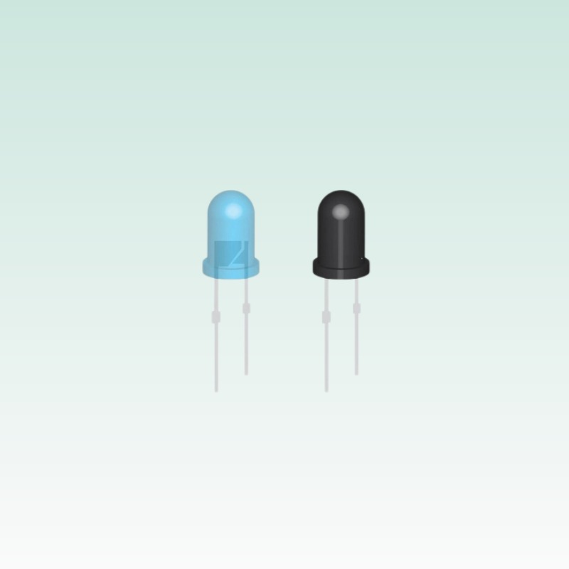
5.3 DIP with epoxy lens (5 mm, 3 mm)
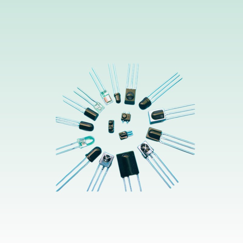
The epoxy lens is both the optical element and the environmental seal. Under blue or UV photons it yellows, and because the lens is the light extraction path, yellowing degrades both flux and colour. The long wire loop typical of DIP construction also makes wire fatigue the second mechanism. J-04 (5 mm IR) and J-10 (3 mm UVA) are the representative parts; for long-life indicator duty, specify a silicone-lens equivalent where available.
5.4 UV ceramic (J-15 UVC 275 nm, Z-14 lamp tubes)
Ultraviolet photons break polymer bonds directly, so any organic material in the optical path degrades. The failure mode is seal degradation and encapsulant haze rather than sulfurization. Note the strict separation of technologies: J-15 is a 275 nm UV-C LED chip, while Z-14 is a 254 nm / 365 nm mercury-lamp tube; their failure mechanisms and replacement economics are entirely different and must not be conflated in a specification or a warranty discussion.
6. Avoidance by design review
The most effective failure analysis is the one that never becomes necessary. A design review checklist based on this atlas:
- Match the anti-sulfur specification to the installation environment, not to the laboratory.
- Verify that the MCPCB stack-up used in qualification matches the production stack-up.
- Confirm that the ESD control programme meets IEC 61340-5-1 at every handling station, and that the LED part’s HBM classification is stated on the datasheet.
- For UV paths, eliminate organic adhesives and gaskets from the optical aperture.
- For pulsed or dimmed applications, verify that peak current and duty cycle stay inside the package’s pulse rating, not merely inside the average-current rating.
- Require LM-80 data at a case temperature at or above the application’s expected case temperature.
7. Verification and reporting
A completed failure analysis report should state the observed symptom, the stages performed, the confirmed mechanism, the estimated root-cause process or design factor, and the corrective action with its verification method. A report that stops at “the LED failed” is not an analysis. Where the mechanism is thermal or mechanical, the report should include the accelerated test that reproduces it, so that the corrective action can be validated on new material.
8. Conclusion
Package type is a strong prior for failure mechanism: plastic SMD fails on sulfur and moisture, ceramic high-power fails on mechanical interfaces, DIP fails on its lens, and UV devices fail on their seal. Starting from that prior and narrowing with electrical, optical and physical tests in cost order produces a defensible root cause quickly and avoids both over-testing and premature conclusions.
9. Referenced standards
- JESD22 — JEDEC solid state reliability test methods (A104 thermal shock, A105 power cycling)
- JESD91 — Method for developing acceleration models for electronic component failure mechanisms
- ANSI/ESDA/JEDEC JS-001 — Human body model component level testing
- IEC 61340-5-1 — Protection of electronic devices from electrostatic phenomena
- IEC 60068-2-43 — Hydrogen sulphide test
- IES LM-80 — Luminous flux maintenance testing
10. Contact us
QUEENDOM’s component engineering group supports field returns with electrical screening, C-SAM imaging, decapsulation and SEM/EDS analysis. Provide the application environment, drive conditions and a sample of the failed board so that the analysis can account for the board stack-up and thermal path.
Failure-Mode Distribution Across Package Families
Knowing which mechanism dominates for each package is the difference between a two-day diagnosis and a two-week one. The curves below summarise field-return statistics for our SMD, DIP, ceramic and COB families. The first orders mechanisms by share of returns; the second shows how the dominant mechanism shifts as junction temperature rises.
Figure 1 – Share of field returns by dominant failure mechanism, split by package family. Representative service data.
Across the combined return population, sulfurization and encapsulant issues account for the majority of SMD returns, while wire-bond and die-attach fatigue dominate ceramic high-power parts. This is expected: the SMD family is used in open, frequently sulfur-bearing environments, whereas ceramic parts run at higher current densities where thermo-mechanical cycling drives the failure.
Figure 2 – Relative risk index for chemical versus thermo-mechanical mechanisms against junction temperature. Representative model for triage guidance.
The practical use of these curves is triage order. For an SMD return, inspect the reflector silver first; for a ceramic high-power return, start with thermal-interface and wire-bond integrity. Our SMD LED, high-power and through-hole families are each characterised under the mechanism that dominates their population, so the diagnosis follows the package rather than the symptom.
Related products and applications
The packages covered by this failure-mode atlas are available in the following families.