
 English
 Afrikaans
 Albanian
 Amharic
 Arabic
 Armenian
 Azerbaijani
 Basque
 Belarusian
 Bengali
 Bosnian
 Bulgarian
 Catalan
 Cebuano
 Chichewa
 Corsican
 Croatian
 Czech
Czech Danish
 Dutch
Dutch Esperanto
 Estonian
 Filipino
 Finnish
 French
 Frisian
 Galician
 Georgian
 German
 Greek
Greek Gujarati
 Haitian Creole
 Hausa
Hausa Hawaiian
 Hebrew
 Hindi
Hindi Hmong
Hmong Hungarian
 Icelandic
 Igbo
Igbo Indonesian
 Irish
Irish Italian
 Japanese
 Javanese
 Kannada
 Kazakh
 Khmer
Khmer Korean
 Kurdish (Kurmanji)
 Kyrgyz
 Lao
Lao Latin
Latin Latvian
 Lithuanian
 Luxembourgish
 Macedonian
 Malagasy
 Malay
Malay Malayalam
 Maltese
 Maori
Maori Marathi
 Mongolian
 Myanmar (Burmese)
 Nepali
 Norwegian
 Pashto
 Persian
 Polish
 Portuguese
 Punjabi
 Romanian
 Russian
 Samoan
 Scottish Gaelic
 Serbian
 Sesotho
 Shona
Shona Sindhi
 Sinhala
 Slovak
 Slovenian
 Somali
 Spanish
 Sudanese
 Swahili
 Swedish
 Tajik
Tajik Tamil
Tamil Telugu
 Thai
Thai Turkish
 Ukrainian
 Urdu
Urdu Uzbek
Uzbek Vietnamese
 Welsh
Welsh Xhosa
Xhosa Yiddish
 Yoruba
 Zulu
Zulu







LED Failure Analysis Knowledge Base
Comprehensive failure analysis resources covering SMD, DIP, infrared, display, and ESD failure modes — based on 25+ years of manufacturing and field service data from Queendom’s global LED installations.
Why LED Failure Analysis Matters
Understanding LED failure modes is critical for product reliability, quality control, and field service. Unlike many electronic components, LEDs degrade gradually rather than failing instantaneously, making root cause analysis challenging without specialized knowledge and equipment. This knowledge base provides engineers, technicians, and quality assurance professionals with the diagnostic tools and prevention strategies needed to minimize LED field failures.
Our failure analysis database is organized by package type and failure mechanism. Each section provides: (1) detailed description of the failure mode and its root cause, (2) detection and diagnostic methods, (3) real-world case studies from field returns (sanitized to protect customer confidentiality), (4) prevention strategies for design and manufacturing, and (5) frequently asked questions from engineering teams.
Failure Analysis Categories
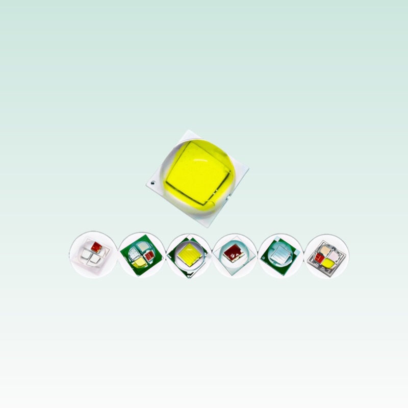
High-Power LED Failure Analysis
Ceramic high-power LED (1W–30W) failure modes: thermal fatigue, die-attach delamination, wire bond lift-off, phosphor degradation, and EOS/ESD
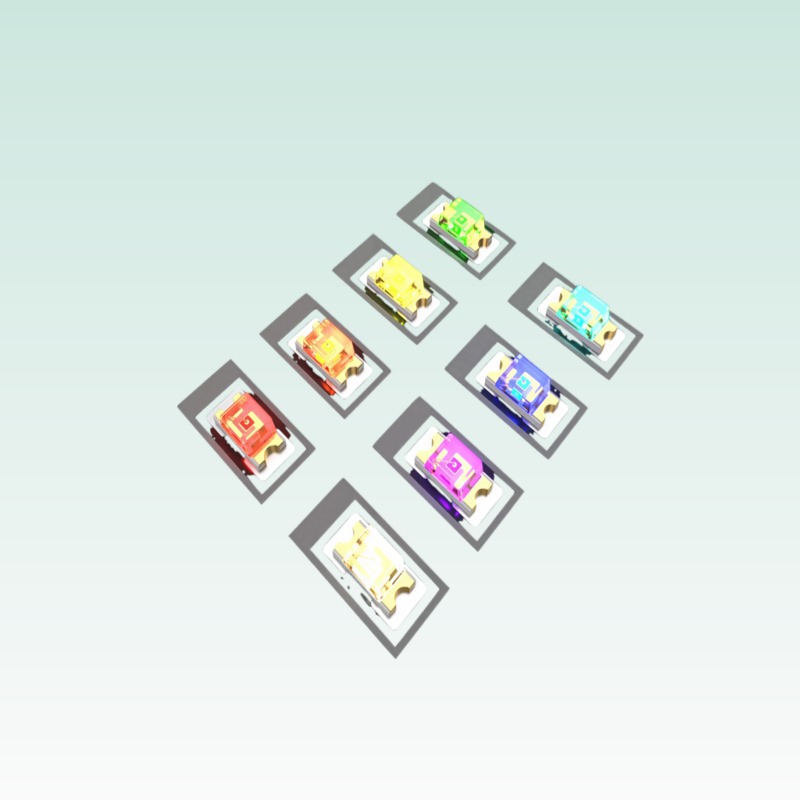
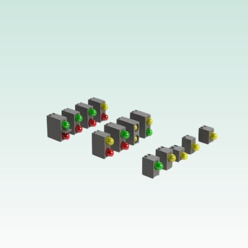
SMD LED Failure Analysis
Solder joint defects, thermal degradation, EOS/ESD damage in surface-mount packages
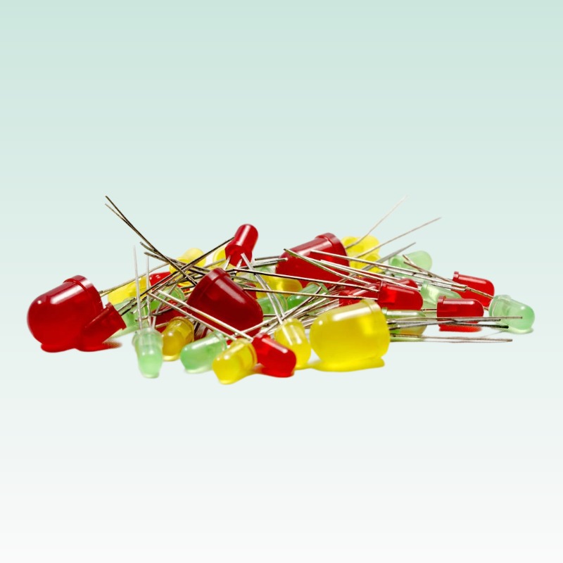
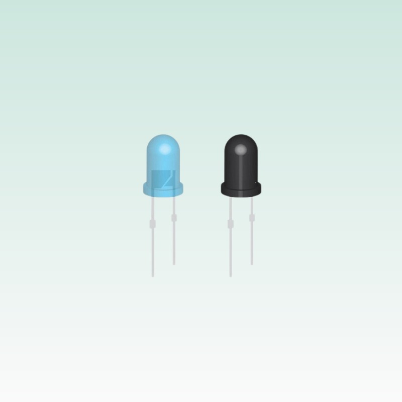
DIP LED Failure Analysis
Lead corrosion, wire bond failure, epoxy degradation in through-hole packages
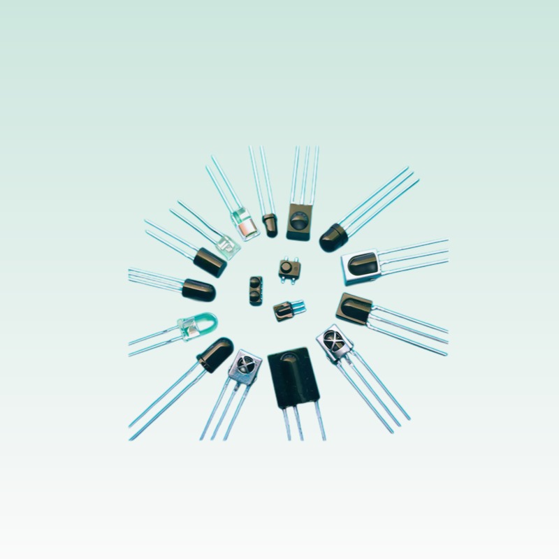
IR LED Failure Analysis
Wavelength shift, radiant intensity degradation, encapsulation issues in infrared LEDs
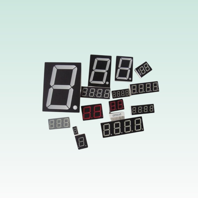
LED Display Failure Analysis
Dead pixels, color shift, water damage, controller issues in LED display modules
ESD Damage and Prevention
HBM/CDM damage mechanisms, protection circuit design, ESD-safe handling procedures
Statistical Overview
Based on our analysis of field-returned LEDs across all product lines over the past 5 years, the distribution of failure modes is:
- Solder joint / interconnect failures: 35% — primarily in SMD assemblies with inadequate thermal management
- ESD/EOS damage: 22% — concentrated in dry-climate installations and automated assembly environments
- Thermal degradation: 18% — high-power applications with insufficient heat sinking
- Environmental damage: 15% — moisture, sulfur, UV exposure in outdoor and industrial applications
- Manufacturing defects: 10% — die-level defects, wire bond issues, encapsulation problems
For detailed analysis of each failure mode, select the relevant category above. If you need application-specific failure analysis support, contact our engineering team through the Customer Support Center.
How a Failure Analysis Actually Runs
A disciplined analysis moves from non-destructive to destructive, because every cut destroys evidence. Our standard sequence:
- Intake and history — lot code, drive conditions, board schematic, failure rate per million hours, and whether the failure is dead-on-arrival, gradual, or catastrophic
- Non-destructive inspection — optical microscopy at 50×–200×, electrical curve tracing (I-V and reverse leakage), and X-ray to see wire bonds, die attach voids, and package cracks
- Scanning acoustic microscopy (SAM) — maps delamination between die, encapsulant, and substrate without opening the package
- Destructive analysis — decapsulation or cross-section, then SEM/EDX on the failure site to identify foreign elements, intermetallics, or contamination
- Root-cause verdict — classified as die-level, package-level, or application-level, with a corrective action routed to the responsible process For luminaire-level symptoms — dead fixtures, flicker, nuisance trips, sensor faults — start instead from the lighting troubleshooting guide, which routes whole-fixture problems separately from component failures.
Failure Signature Reference
Field symptoms cluster into recognizable signatures. Use this table as a first-pass triage before a part ships to the lab:
| Observed Symptom | Most Likely Root Cause | First Response |
|---|---|---|
| Dead on arrival, no light, low reverse leakage | Open wire bond or ESD-damaged junction | Check ESD controls at the assembly station; X-ray the bond |
| Dead on arrival, low resistance both directions | Die short (EOS or reverse overvoltage) | Review drive circuit transients and reverse-bias conditions |
| Gradual lumen depreciation | Junction overtemperature, undersized thermal path | Measure case temperature under load; improve heatsinking or derate |
| Color shift toward yellow/dark output | Encapsulant yellowing from heat or UV exposure | Verify operating temperature; for UVA parts review duty cycle |
| Flicker or intermittent contact | Cracked solder joint, flexing PCB, or intermittent bond | Micro-section the joint; check board support near the LED |
| Catastrophic package crack | Thermal shock or moisture popcorning in reflow | Audit MSL handling and bake before reflow |
| Corrosion on leads | Chlorine or sulfur atmosphere (coastal, industrial) | Specify conformal coating or resistant-finish packages |
Prevention by Design Stage
The cheapest failure analysis is the one you never run. Route prevention into the design review: derate forward current to 70–80% of maximum for long-life products; size the thermal path for worst-case ambient, not typical; select MSL-rated packages matched to your floor’s exposure time; and run pre-production ESD audits at every human touch point. During NPI, a 168-hour HTOL sample and a 100-cycle thermal-shock sample catch the infant-mortality population before it ships. These measures cost hours; field recalls cost months — a tradeoff documented across the reliability sections of our certification documentation.
Frequently Asked Questions
What should I send with a failed LED sample?
Send the failed part unsoldered if possible, plus two known-good parts from the same lot, the datasheet revision you designed to, and the measured drive conditions (current, duty cycle, ambient). Context turns a week of guessing into a day of analysis.
Can ESD damage be confirmed after the fact?
Often yes. ESD leaves a recognizable signature: a puncture or melt filament in the junction visible after decapsulation, with electrical evidence of a soft resistive path. The damage is usually near a bond pad on the discharge side.
My failure rate is 200 ppm — is that good?
For assembled consumer products, under 50 ppm is the common target and 200 ppm warrants a formal 8D. For automotive-grade programs, plan for single-digit ppm with 0 km and field-return tracking separated.
How long does a full analysis take?
Electrical and optical triage completes in 2–3 working days; a full destructive sequence with SEM/EDX runs 1–2 weeks depending on lab queue. Report format follows the 8D structure with containment, root cause, and corrective action tracking.