











An infrared illuminator that works perfectly on the bench at 25 °C can lose a third of its radiant output once the same LEDs are mounted in a sealed camera housing in the sun. Nothing has failed. The LEDs are simply hotter, and infrared LEDs lose output with temperature faster than most visible-light parts, because the radiative recombination efficiency in the active region falls as the junction warms. Engineers who treat junction temperature as a datasheet footnote discover this at the worst possible moment, during commissioning of a machine-vision or surveillance system. This page sets out the temperature dependence of near-infrared LED output, the thermal resistance chain that determines the junction temperature, and the drive-current decisions that set the operating point. It is written for machine vision engineers, surveillance system designers, sensing and photometry specialists, and buyers writing performance specifications for infrared emitters.
1. Why infrared output is more temperature-sensitive than visible output
In a visible-white LED, a portion of the emitted light comes from a phosphor that is relatively insensitive to moderate temperature change, so the overall output falls relatively gently. In a direct-emission infrared LED at 850 nm, 880 nm or 940 nm, there is no phosphor and no second mechanism: the output is the electroluminescence of the AlGaAs or InGaAs active region, and that output falls monotonically as the junction temperature rises. The temperature coefficient is conventionally expressed as a percentage change in radiant flux per kelvin, and for near-infrared emitters it typically lies between -0.4 %/K and -0.8 %/K, a range that is both significantly steeper and significantly more variable than for visible emitters of comparable power.
Two consequences follow for the system designer. First, the junction temperature must be computed rather than assumed, and the value used in any lifetime or performance projection must be the one that occurs in the installed environment, not the one measured on an open bench. Second, because the LED’s own output falls as the junction warms, the initial optical design carries a thermal penalty that compounds: a marginal heat sink does not merely reduce lifetime, it reduces the illumination the system delivers on day one.
The relevant wavelength separation also matters for the application. Near-infrared emitters at 850 nm, 880 nm and 940 nm are the workhorses of night vision, covert illumination, machine vision at silicon sensor wavelengths, and proximity sensing. Short-wave infrared at 1600 nm and 2000 nm belongs to a different material system and a different application class, and the two must not be conflated in a specification or a thermal design.
| Parameter | 850 nm class | 880 nm class | 940 nm class |
|---|---|---|---|
| Typical application | CCTV, machine vision, illumination | Sensing, industrial vision | Covert illumination, proximity, eye-safe sensing |
| Silicon sensor response | High | Moderate to high | Low (also low solar background) |
| Output versus Tj coefficient | -0.4 to -0.6 %/K | -0.5 to -0.7 %/K | -0.6 to -0.8 %/K |
| Visible red leakage | Small but present | Very small | Essentially none |
| Forward voltage, typical | 1.6–2.2 V | 1.5–2.0 V | 1.2–1.8 V |
| Radiant efficiency | Highest of the three | Mid | Lowest of the three |
| Thermal sensitivity rank | Lowest | Mid | Highest |
2. The thermal path: from junction to ambient
Junction temperature is not a measured quantity in normal operation; it is calculated. The standard relation is:
Tj = Ta + Rj-a × Pd
where Ta is the ambient temperature, Rj-a is the total thermal resistance from junction to ambient, and Pd is the electrical power dissipated in the device, which for an LED is dominated by the total electrical power less the emitted optical power. Because near-infrared LEDs typically convert 30–50 % of the electrical input into useful radiant flux, the dissipated power is not equal to the product of forward voltage and forward current; the optical power must be subtracted, or the junction temperature will be overestimated.
The total thermal resistance is a series sum along the heat path, and each element in the chain contributes:
Rj-a = Rj-sp + Rsp-b + Rboard + Rinterface + Rheatsink + Rconv
with a junction-to-solder-point term inside the package, a solder-point-to-board term, an in-plane and through-plane board spreading term, a thermal interface material term, a heat sink term, and a convection or radiation term to ambient. The important engineering insight is that no single term dominates for a well-designed board, so improving only one element yields a less than proportional improvement — halving the heat sink resistance when it is one of six comparable terms changes the junction temperature by less than the naive estimate suggests.
| Path element | Symbol | Typical range | Dominated by | Design lever |
|---|---|---|---|---|
| Junction to solder point | Rj-sp | 4–12 K/W | Package construction, die attach | Choose ceramic package for high power |
| Solder point to board | Rsp-b | 2–8 K/W | Solder voiding, pad area | Control reflow, use a full thermal pad |
| Board spreading | Rboard | 5–30 K/W | Copper area, thickness, layer count | Maximise copper, use thermal vias |
| Interface material | Rinterface | 0.5–3 K/W | TIM thickness and conductivity | Thin bond line, correct TIM |
| Heat sink to air | Rheatsink | 2–20 K/W | Material, geometry, airflow | Larger area, forced air if needed |
| Convection to ambient | Rconv | 5–40 K/W | Airflow, orientation, enclosure | Ventilation, orientation, avoid dead air |
3. Junction temperature versus output
The relationship between output and junction temperature is close to linear over the useful range, which is why the coefficient is quoted as a percentage per kelvin. Over a wider range it curves, and at high junction temperatures the decline steepens as non-radiative recombination and other loss mechanisms grow faster than the radiative path.
The practical implication is that thermal design and optical design are the same task for infrared systems. Selecting a 940 nm emitter to reduce visible red leakage, and then accepting a junction temperature 30 K higher than the 850 nm alternative would have reached, can leave the system with less usable irradiance at the target than the 850 nm part delivered.
| Junction temperature | 850 nm output | 880 nm output | 940 nm output | Application note |
|---|---|---|---|---|
| 25 °C | 100 % | 100 % | 100 % | Reference condition, bench measurement |
| 50 °C | 89 % | 86 % | 83 % | Typical open luminaire |
| 75 °C | 78 % | 73 % | 66 % | Sealed enclosure with modest heat sinking |
| 100 °C | 68 % | 60 % | 50 % | Poorly ventilated housing, high drive current |
| 125 °C | 58 % | 48 % | 36 % | At or beyond the recommended maximum |
4. Drive current, forward voltage and the operating point
Drive current affects the junction temperature in two ways, and the interaction is the most common source of over-optimistic design. The first effect is direct: increasing the current increases the electrical power dissipated, which raises the junction temperature. The second effect is subtler: for LEDs, the forward voltage at a given current typically falls as the junction temperature rises, so the device can draw slightly more current for a given applied voltage as it heats, in a feedback loop that is limited only by the drive circuit topology. Constant-current drive breaks this loop; constant-voltage drive does not, and is a common cause of thermal runaway in poorly designed infrared illuminators.
The optical efficiency of the emitter also falls with current, a phenomenon often called droop. Going from 1 A to 2 A in a typical infrared emitter may increase radiant output by only 60–80 %, not by 100 %, while doubling the dissipated heat. Combined with the negative temperature coefficient, the marginal gain per additional ampere is small, and beyond a certain point the added heat can make the total usable output fall.
The convergence of the curves at high junction temperature is the key design lesson. Increasing the drive current buys output only while the thermal path can carry the additional heat away. Once the operating point is pushed into the region where the curves meet, the additional current produces more heat and no more usable light.
| Drive current | Vf, typical | Electrical power | Radiant power at 25 °C | Estimated Tj, Rj-a = 25 K/W | Radiant power at that Tj |
|---|---|---|---|---|---|
| 350 mA | 1.9 V | 0.67 W | 240 mW | 42 °C | 219 mW |
| 650 mA | 2.1 V | 1.37 W | 450 mW | 66 °C | 381 mW |
| 1,000 mA | 2.3 V | 2.30 W | 610 mW | 92 °C | 467 mW |
| 1,500 mA | 2.6 V | 3.90 W | 780 mW | 130 °C | 466 mW |
Note the plateau between 1,000 mA and 1,500 mA in the final column. At the assumed thermal resistance, driving the emitter harder than about 1 A adds heat without adding usable output. The exact current at which this occurs is set by the thermal resistance, which is why the thermal design must be settled before the drive current is chosen, and not the other way round.
5. Measuring junction temperature properly
Junction temperature is measured indirectly, and the choice of method determines whether the number is meaningful for an installed fixture.
The forward-voltage method uses the calibrated temperature coefficient of Vf. The device is characterised on a temperature-controlled stage to establish the Vf-versus-temperature slope at a fixed, low measurement current; it is then operated at the target current until thermal equilibrium is reached, the current is momentarily switched to the measurement value, and Vf is read and converted to a temperature. The switching must be fast enough that the junction does not cool during the measurement. This method gives the true junction temperature and is the reference method described in JESD51-1 and JESD51-14.
The transient thermal analysis method measures the thermal impedance curve by applying a step in power and recording the junction temperature response over time. This yields not just a single temperature but the cumulative structure function of the thermal path, which lets the engineer identify where in the chain the resistance actually lies. It is the correct tool when a design is not meeting its thermal target and the cause is unknown.
The thermal imaging method reads the package surface, not the junction. It is useful for finding gross layout problems and for confirming that the board spreads heat as intended, but it systematically underestimates junction temperature because the junction is inside the package and separated from the visible surface by thermal resistance. It should never be used as the basis of a lifetime projection.
| Method | Output | Accuracy | Effort | Appropriate use |
|---|---|---|---|---|
| Forward voltage method | True junction temperature | High, if calibrated | Moderate | Reference measurement, qualification |
| Transient thermal analysis | Junction temperature plus path structure | High | High | Diagnosing an unmet thermal target |
| Thermal imaging of package | Surface temperature | Low for Tj | Low | Layout screening, fault finding |
| Thermocouple on solder point | Solder point temperature | Moderate | Low | Production verification with a known Rj-sp |
| Thermal simulation | Predicted junction temperature | Depends on model validation | High | Design stage, before hardware exists |
6. Product family and selection guidance
| Part | Type | Wavelengths | Package | Typical drive | Thermal note |
|---|---|---|---|---|---|
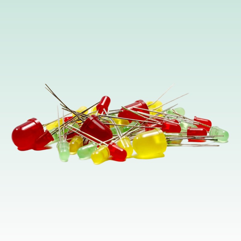
| J-04 | 5 mm DIP infrared | 850 / 880 / 940 nm | Epoxy lens DIP | 20–100 mA | Low power, epoxy lens limits continuous rating; poor Rj-a |
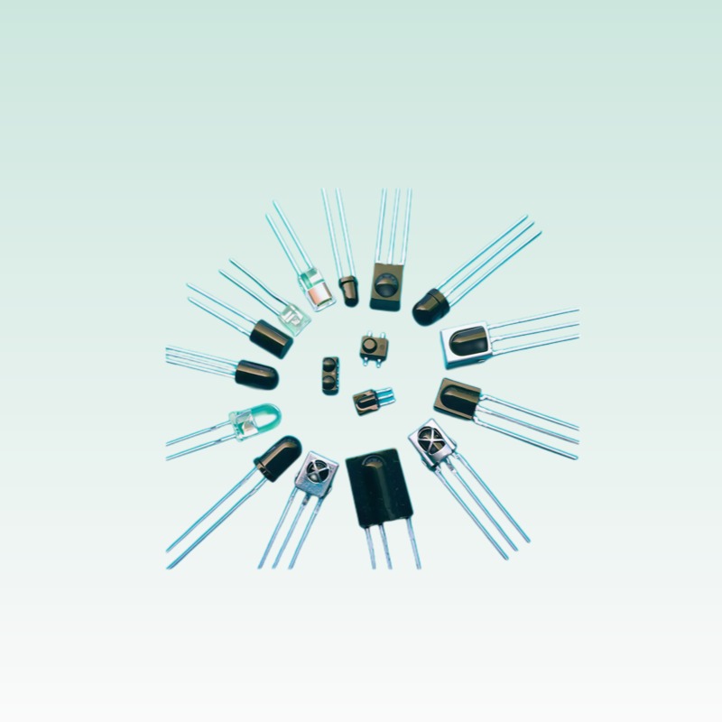
| J-05 | 2835 infrared | 850 / 880 / 940 nm | 2835 plastic SMD | 150–700 mA | Volume part; thermal path depends entirely on the board copper |
| J-06 | 3535 infrared | 730 / 850 / 940 nm | 3535 SMD | 350–1,000 mA | Best thermal path of the three; preferred for high-irradiance arrays |
| J-12 | 3535 UVA | 365 / 375 / 385 nm | 3535 SMD | 350–1,000 mA | Comparable thermal behaviour, different application |
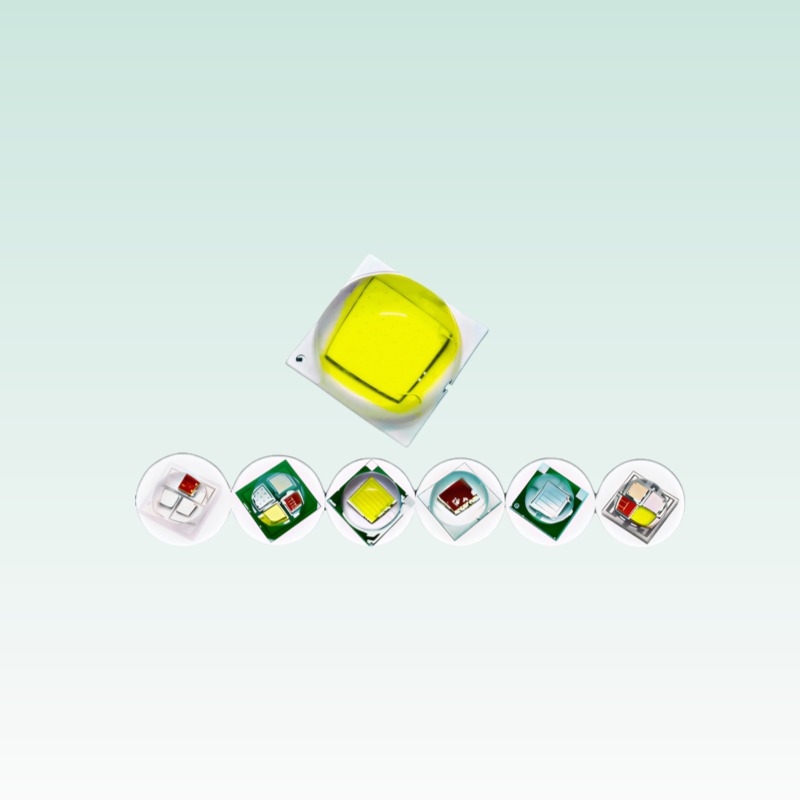
| J-01 | 3535 ceramic, visible | Visible high power | 3535 AlN ceramic | 350–1,500 mA | Ceramic body gives the lowest Rj-sp of the family |
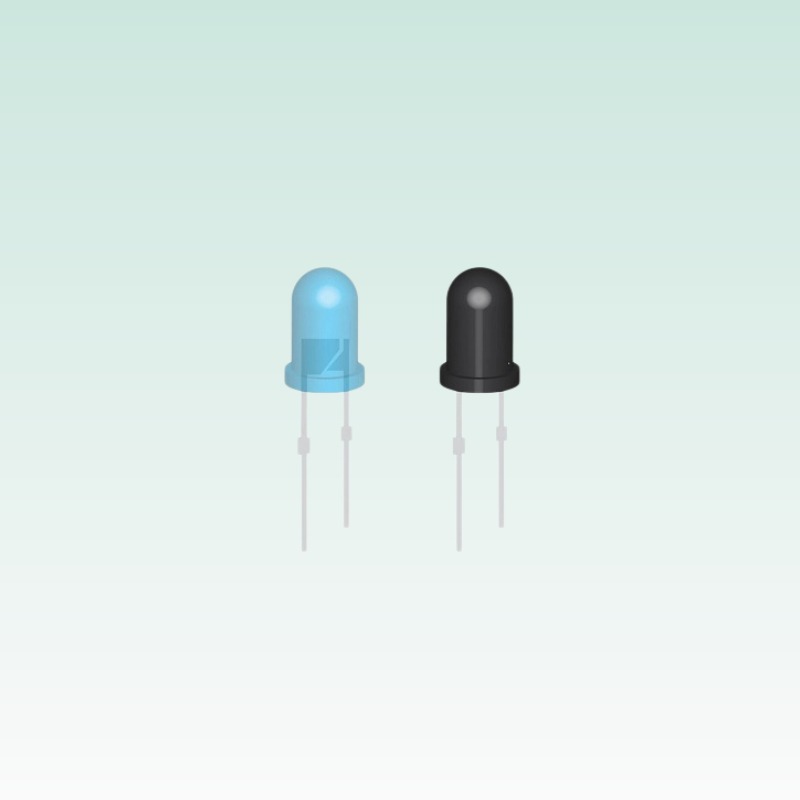
The choice between the three infrared parts is largely a thermal choice. J-04 (5 mm DIP infrared, 850 / 880 / 940 nm) is a low-power indicator and sensing device whose epoxy lens and lead-frame construction give a high thermal resistance, so continuous high-current operation is not appropriate; it is suited to pulsed operation at modest duty. J-05 (2835 infrared, 850 / 880 / 940 nm) is the volume part, and its junction temperature is determined almost entirely by the copper area underneath it, which means the same part can run 30 K cooler or hotter depending on the board design. J-06 (3535 infrared, 730 / 850 / 940 nm) offers the best thermal path of the three and is the appropriate choice for high-irradiance arrays where several watts must be extracted, and it adds 730 nm for applications requiring a deeper red component.
Note also that the 730 nm wavelength in J-06 sits at the boundary between the visible and near-infrared, and that the higher-wavelength short-wave infrared emitters at 1600 nm and 2000 nm in this portfolio are a separate material system with separate thermal and optical characteristics.
7. Common errors and how to avoid them
| Error | Consequence | Correct approach |
|---|---|---|
| Using ambient temperature as the junction temperature | Output overestimated by 30–50 % | Calculate Tj from Rj-a and dissipated power |
| Substituting electrical power for dissipated power | Tj overestimated, radiative part ignored | Subtract radiant output from electrical input |
| Driving at constant voltage | Thermal runaway, current rises with temperature | Use a constant-current driver |
| Selecting a heat sink in isolation | Mixed path, less improvement than expected | Optimise the whole Rj-a chain, not one element |
| Measuring Tj with a thermal camera | Surface is cooler than the junction | Use the forward-voltage or transient method |
| Assuming the output coefficient is the same at all wavelengths | 940 nm part underperforms the design | Use the wavelength-specific coefficient |
| Ignoring the droop at high current | Added current adds heat, not light | Establish the thermal limit before raising the current |
| Designing the thermal path for lifetime only | Initial output already below the target | Design the thermal path for the output target |
| Bench-testing in open air | Installed fixture runs 40 K hotter | Test in the production enclosure |
8. Worked example
Consider a machine-vision illuminator using J-06 (3535 infrared, 850 nm) at 1 A, with the target of delivering at least 400 mW of usable radiant flux at the working plane in an enclosure that reaches 45 °C internally.
The package’s junction-to-solder-point resistance is taken as 8 K/W. The board, with 400 mm² of copper and thermal vias, contributes 12 K/W. The thermal interface material contributes 1.5 K/W, and the heat sink with natural convection in the sealed enclosure contributes 18 K/W, giving a total Rj-a of 39.5 K/W. At 1 A the forward voltage is 2.3 V, giving 2.3 W of electrical input, of which about 0.61 W is emitted as radiant flux at 25 °C, so the dissipated power is 1.69 W. The junction temperature is therefore 45 + 39.5 × 1.69 ≈ 112 °C. At that junction temperature, applying the -0.5 %/K coefficient relative to 25 °C gives a radiant output of about 0.61 × (1 – 0.005 × 87) ≈ 0.345 W, which is below the 400 mW target.
The corrective options are now quantifiable. Reducing the drive current to 650 mA lowers the electrical input to 1.37 W and the dissipated power to about 0.99 W, which brings the junction temperature to 45 + 39.5 × 0.99 ≈ 84 °C; the radiant output at 650 mA falls from 0.45 W at 25 °C to about 0.45 × (1 – 0.005 × 59) ≈ 0.317 W, still short of the target. Improving the heat sink from 18 K/W to 8 K/W lowers the total Rj-a to 29.5 K/W, which at 1 A gives a junction temperature of 45 + 29.5 × 1.69 ≈ 95 °C and an output of about 0.61 × (1 – 0.005 × 70) ≈ 0.397 W. Combining the lower thermal resistance with two emitters at 650 mA each delivers the target, which is why illuminator arrays are usually designed by thermal budget rather than by single-emitter output.
| Scenario | Rj-a (K/W) | I (mA) | Pd (W) | Tj (°C) | Radiant output (mW) | Meets 400 mW? |
|---|---|---|---|---|---|---|
| Baseline, single emitter at 1 A | 39.5 | 1,000 | 1.69 | 112 | 345 | No |
| Reduced current, same heat sink | 39.5 | 650 | 0.99 | 84 | 317 | No |
| Improved heat sink, 1 A | 29.5 | 1,000 | 1.69 | 95 | 397 | Marginal |
| Improved heat sink, two emitters at 650 mA | 29.5 each | 650 each | 0.99 each | 74 | 2 × 353 = 706 | Yes |
| Improved heat sink, forced air, 1 A | 22 | 1,000 | 1.69 | 82 | 436 | Yes |
9. Verification and reporting
A supplier’s infrared output figure is only useful when it comes with the two conditions that determine it: the junction temperature and the drive current. A datasheet that quotes radiant flux at an unspecified case temperature, or at a case temperature far below the application’s, cannot be used directly in a system design. The specification should require radiant flux against a drive current and a defined thermal condition, the Vf-versus-temperature coefficient, the temperature coefficient of radiant flux for the specific wavelength, the package’s junction-to-solder-point thermal resistance, and the maximum rated junction temperature. Where a lifetime figure is quoted, it should follow the LM-80 and TM-21 format with the case temperature stated, and where automotive relevance is claimed, note that the qualification status is AEC-Q102 in progress, supported by thermal and reliability data rather than by a certificate.
10. Referenced standards
- JESD51-1 — Integrated circuit thermal measurement method: electrical test method, junction temperature measurement
- JESD51-14 — Transient dual interface test method for the measurement of the thermal resistance junction-to-case
- JESD51-51 — Implementation of the electrical test method for the thermal measurement of power LEDs
- IES LM-80-21 — Approved method: measuring luminous flux and colour maintenance of LED packages, arrays and modules
- IES TM-21-19 — Projecting long term lumen maintenance of LED light sources
- JESD22-A104 — Temperature cycling
- JESD22-A101 — Steady state temperature humidity bias life test
- IEC 62471 — Photobiological safety of lamps and lamp systems
- AEC-Q102 — Stress test qualification for automotive discrete optoelectronic semiconductors
- IEC 60529 — Degrees of protection provided by enclosures (IP Code)
11. Contact us and sample requests
QUEENDOM supplies the 5 mm DIP infrared part (J-04, 850 / 880 / 940 nm), the 2835 infrared part (J-05, 850 / 880 / 940 nm) and the 3535 infrared part (J-06, 730 / 850 / 940 nm), together with thermal characterisation data and drive-condition data for system design. When requesting samples or design support, state the installed ambient temperature inside the enclosure, the available board copper area and stack-up, the drive topology, the duty cycle, and the required irradiance at the target distance, so that the thermal resistance chain can be evaluated against the application rather than against a bench measurement and the correct emitter and drive condition selected.
Related products and applications
The infrared emitters referenced in this depreciation study are listed below.
- Infrared emitter LED (J-04)
- Infrared emitter LED (J-05)
- Infrared emitter LED (J-06)
- Application overview: LED components application solutions
- More technical papers: LED knowledge resources