
 English
 Afrikaans
 Albanian
 Amharic
 Arabic
 Armenian
 Azerbaijani
 Basque
 Belarusian
 Bengali
 Bosnian
 Bulgarian
 Catalan
 Cebuano
 Chichewa
 Corsican
 Croatian
 Czech
Czech Danish
 Dutch
Dutch Esperanto
 Estonian
 Filipino
 Finnish
 French
 Frisian
 Galician
 Georgian
 German
 Greek
Greek Gujarati
 Haitian Creole
 Hausa
Hausa Hawaiian
 Hebrew
 Hindi
Hindi Hmong
Hmong Hungarian
 Icelandic
 Igbo
Igbo Indonesian
 Irish
Irish Italian
 Japanese
 Javanese
 Kannada
 Kazakh
 Khmer
Khmer Korean
 Kurdish (Kurmanji)
 Kyrgyz
 Lao
Lao Latin
Latin Latvian
 Lithuanian
 Luxembourgish
 Macedonian
 Malagasy
 Malay
Malay Malayalam
 Maltese
 Maori
Maori Marathi
 Mongolian
 Myanmar (Burmese)
 Nepali
 Norwegian
 Pashto
 Persian
 Polish
 Portuguese
 Punjabi
 Romanian
 Russian
 Samoan
 Scottish Gaelic
 Serbian
 Sesotho
 Shona
Shona Sindhi
 Sinhala
 Slovak
 Slovenian
 Somali
 Spanish
 Sudanese
 Swahili
 Swedish
 Tajik
Tajik Tamil
Tamil Telugu
 Thai
Thai Turkish
 Ukrainian
 Urdu
Urdu Uzbek
Uzbek Vietnamese
 Welsh
Welsh Xhosa
Xhosa Yiddish
 Yoruba
 Zulu
Zulu
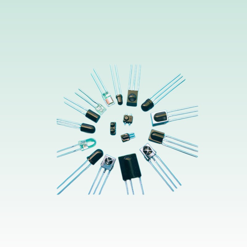
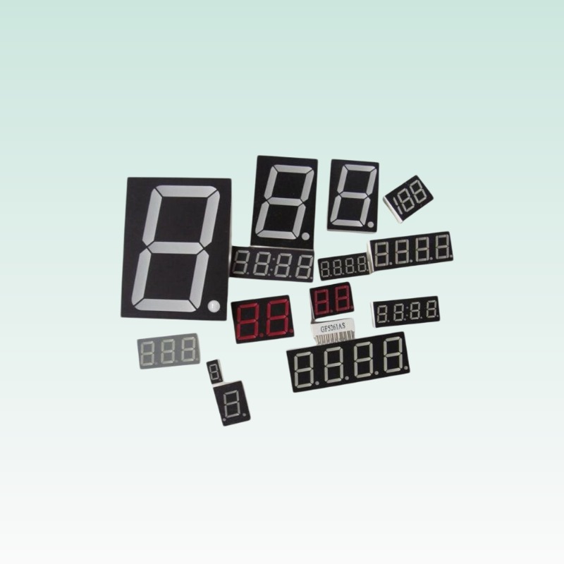
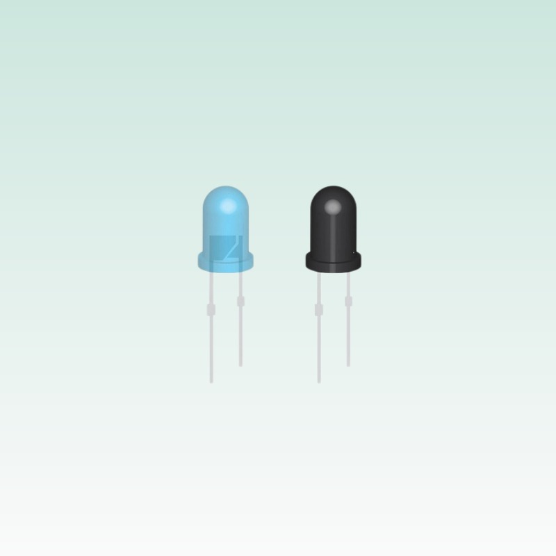
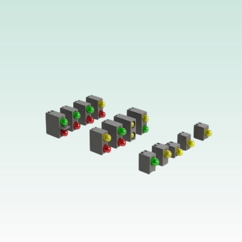







Design Resources
Access 3D mechanical models, PCB footprints, SPICE electrical models, and reference designs for Queendom LED components. These resources help engineers accelerate product development from prototype to production.
Available Resources
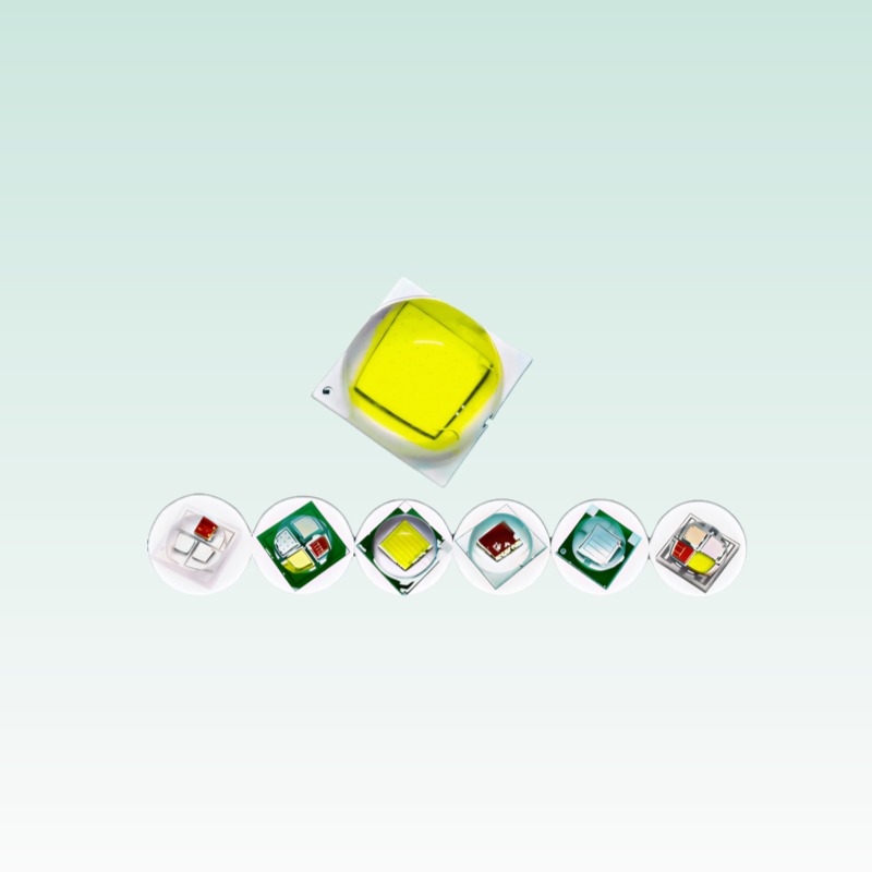
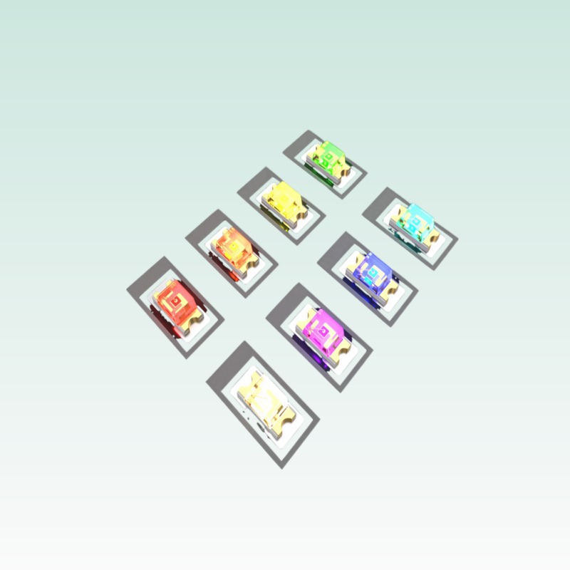
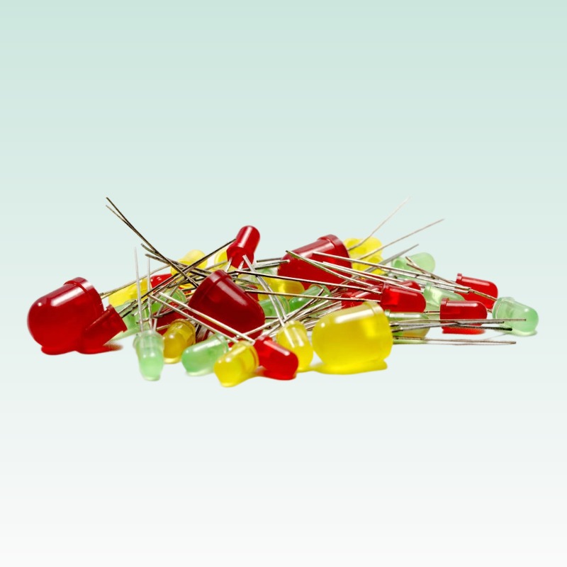
- 3D Mechanical Models — STEP and IGES files for SMD, DIP, and high-power LED packages
- PCB Footprints — Gerber and Altium library files for PCB design
- SPICE Electrical Models — Circuit simulation models for LED behavior prediction
- Reference Designs — Application-specific circuit designs and layout examples
- Optical Ray Data — Ray files for optical simulation software
Related Resources
Datasheets: LED Datasheet Center
Selection: LED Selection Guide
Application Notes: Application Notes
LED Design Engineering Guide
Optical Design
LED optical design starts with the radiation pattern. Datasheets specify the viewing angle (50% intensity angle) and total luminous flux measured under CIE 127 Condition A or B. When selecting a secondary optic or reflector, match the source size to the optic entrance aperture — an oversized LED die in a small reflector produces spill light and beam non-uniformity. For color-critical applications, review the dominant wavelength (λd) bins and chromaticity coordinates (x, y) rather than nominal color names, and request binning limits in writing for production lots.
Thermal Design
Junction temperature is the single most important lifetime factor for LEDs. Estimate it with Tj = Ta + Pdissipated × RθJA, where RθJA is the thermal resistance from junction to ambient through your PCB and heat sink. As a design rule, keep Tj below 100 °C for indicator-class components and below 85 °C for high-power LEDs to protect the phosphor and encapsulant. Our thermal management design guide walks through heat sink sizing, thermal interface material selection, and how LM-80/TM-21 lifetime data maps to your operating temperature.
Electrical Design
LEDs are current-driven devices. Never drive them from a voltage source without current limiting. For a simple DC circuit, size the series resistor as R = (Vsupply − VF) / IF, using the maximum VF from the datasheet bin. For production designs, use a constant-current driver and select the VF bin range carefully — the forward voltage of blue/white/green dies (typically 2.8–3.4 V) differs from red/amber dies (typically 1.9–2.4 V). Add reverse-bias protection (a parallel Schottky diode for AC or reversed-polarity risks) and an ESD protection device at any human-touchable node; most through-hole LEDs are rated only to 2 kV HBM (human body model).
PCB Layout & Soldering
Follow the recommended land pattern in each datasheet — deviations change the solder joint geometry and reliability. For SMD LEDs, design the reflow profile to JEDEC J-STD-020: lead-free peak temperature 245–250 °C for 30–60 seconds, with time above 217 °C kept under 90 seconds. Through-hole DIP LEDs may be wave soldered at 260 °C ±5 °C for a maximum of 5 seconds at the lead. Avoid reworking LEDs more than twice, and never apply mechanical stress to the lens after soldering.
Verification & Testing
Validate your design against the datasheet limits: forward voltage at rated current, luminous intensity or flux at 25 °C, and chromaticity coordinates at thermal steady state (hot/cold factor). For reliability qualification, refer to the standards listed on our LED knowledge hub and request our LM-80 test reports before finalizing the thermal budget.