
 English
 Afrikaans
 Albanian
 Amharic
 Arabic
 Armenian
 Azerbaijani
 Basque
 Belarusian
 Bengali
 Bosnian
 Bulgarian
 Catalan
 Cebuano
 Chichewa
 Corsican
 Croatian
 Czech
Czech Danish
 Dutch
Dutch Esperanto
 Estonian
 Filipino
 Finnish
 French
 Frisian
 Galician
 Georgian
 German
 Greek
Greek Gujarati
 Haitian Creole
 Hausa
Hausa Hawaiian
 Hebrew
 Hindi
Hindi Hmong
Hmong Hungarian
 Icelandic
 Igbo
Igbo Indonesian
 Irish
Irish Italian
 Japanese
 Javanese
 Kannada
 Kazakh
 Khmer
Khmer Korean
 Kurdish (Kurmanji)
 Kyrgyz
 Lao
Lao Latin
Latin Latvian
 Lithuanian
 Luxembourgish
 Macedonian
 Malagasy
 Malay
Malay Malayalam
 Maltese
 Maori
Maori Marathi
 Mongolian
 Myanmar (Burmese)
 Nepali
 Norwegian
 Pashto
 Persian
 Polish
 Portuguese
 Punjabi
 Romanian
 Russian
 Samoan
 Scottish Gaelic
 Serbian
 Sesotho
 Shona
Shona Sindhi
 Sinhala
 Slovak
 Slovenian
 Somali
 Spanish
 Sudanese
 Swahili
 Swedish
 Tajik
Tajik Tamil
Tamil Telugu
 Thai
Thai Turkish
 Ukrainian
 Urdu
Urdu Uzbek
Uzbek Vietnamese
 Welsh
Welsh Xhosa
Xhosa Yiddish
 Yoruba
 Zulu
Zulu
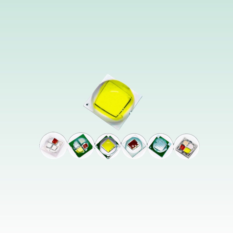

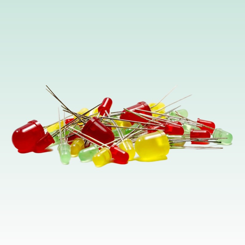
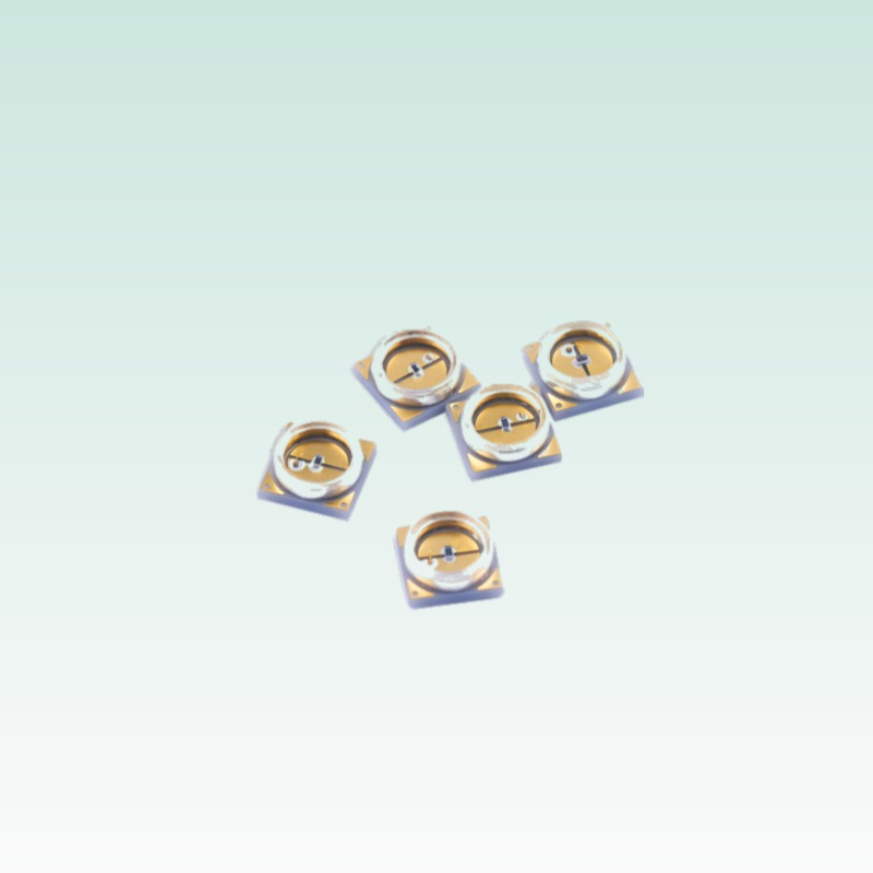
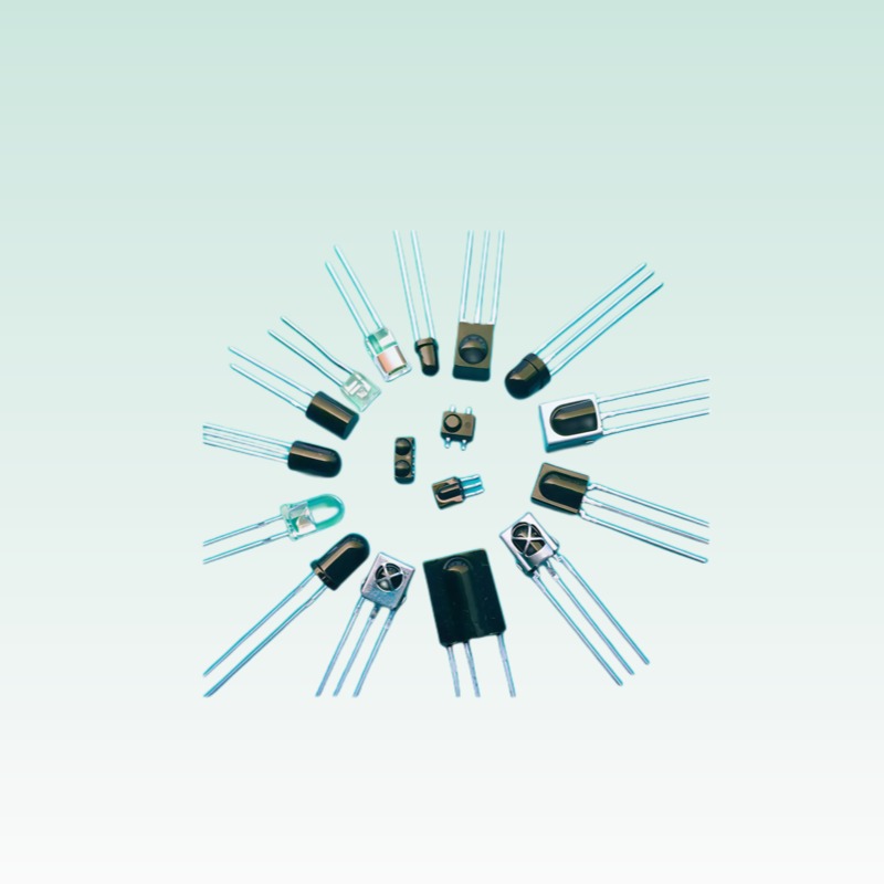








Flip chip LED architecture turns the die upside down: the p-side connects to the submount through an array of solder bumps, and light exits through the transparent substrate instead of the top surface. The wire bond disappears, and with it the weakest link in the reliability chain and a bottleneck in the thermal path. In high-power arrays such as UVA curing heads, SWIR illuminators and ceramic automotive packages, the inversion cuts junction-to-submount thermal resistance by 15-25% and buys back current headroom.
Where the Heat Actually Flows
In a face-up package, the active region sits near the top of the epitaxial stack, above a sapphire substrate 100 µm or thicker. Heat must cross the quantum wells, the GaN layers, the sapphire (thermal conductivity about 35 W/m·K) and the die attach before reaching the copper slug. Wire bonds carry current, not heat, and bond pads block the top surface, so almost nothing escapes upward.
Flip chip collapses that path. The junction now sits only tens of microns above the submount, separated by thin GaN layers and solder bumps. Gold-tin (AuSn) solder, with conductivity near 57 W/m·K, replaces silver-filled epoxy (roughly 7-20 W/m·K) in many designs. The thick sapphire leaves the primary heat path and keeps its job as the light-exit window, while its top face still sheds a secondary heat flow through the encapsulant.
Three Mechanisms, Quantified
Path length: the vertical heat path shrinks from hundreds of microns to tens of microns. A typical 1 mm² face-up package quotes junction-to-solder-point resistance near 10 K/W; flip chip equivalents of the same die size land 15-25% lower, around 7.5-8.5 K/W.
Current spreading: bumps cover the die footprint, so current enters uniformly instead of crowding around a single bond pad. Lower local current density means less local heating and lower effective series resistance, which matters most in large-area UV dies prone to current crowding.
Dual-sided extraction: the substrate face stays open and becomes an auxiliary path into silicone or a lens, useful in dense arrays where neighboring dies share a ceramic board.
| Parameter | Face-up, wire bond | Flip chip |
|---|---|---|
| Heat path to submount | through 100+ µm sapphire | through solder bumps, tens of µm |
| Typical Rth j-sp, 1 mm² die | ~10 K/W | ~7.5-8.5 K/W |
| Bond-wire fatigue risk | present | none |
| Top-side heat extraction | blocked by bond pads | open |
| Minimum die spacing in arrays | set by bond loop height | set by bump pitch |
| Typical service | mid-power, indicators | UV curing, SWIR arrays, AEC-Q102 |
The payoff compounds over life. A 1.5-2.5 K/W saving at 1 A means 1.5-2.5°C less junction rise; degradation rates roughly double every 10°C, so that margin extends L70 lifetime directly. Lower Tj also slows dominant-wavelength shift, typically 0.03-0.05 nm/K for InGaN dies, keeping color or spectral position stable through long duty cycles.
Verifying the Numbers: Tj Measurement
Claims need measurement. The electrical method of JEDEC JESD51-1 calibrates forward voltage as a temperature-sensitive parameter, with a K-factor typically -1 to -2.5 mV/K for InGaN dies, then reads junction rise from a power step. Transient testing per JESD51-14 adds structure-function analysis that separates die, die-attach and board contributions and exposes solder voids as resistance steps.
Package datasheets should quote Rth with test current and reference point; a bare figure is not comparable between suppliers. For lifetime, require LM-80 data at the real drive current and case temperature, extrapolated per TM-21 with its 6× test-duration cap. A flip chip claim without this data chain is a datasheet sentence, not an engineering fact.
Failure Modes That Replace Wire Fatigue
Flip chip removes bond-wire neck fatigue but imports its own failure set: solder bump voids, intermetallic growth at AuSn joints in continuous operation above 150°C, and underfill delamination under thermal cycling. Automotive parts qualify under AEC-Q102. Industrial UV and IR arrays should at minimum cycle -40°C to +125°C and screen bump integrity by X-ray or scanning acoustic microscopy.
FAQ
Q: Does flip chip change the optical design?
Light exits through the substrate side, so optics go above the die and wire-bond clearance disappears. Dies can sit closer together, which is why dense UV COB heads and IR array illuminators favor the format.
Q: How much more current can I run?
With 15-25% lower thermal resistance, the same Tj ceiling allows roughly 15-25% more forward current before derating. The exact gain depends on die size, bump layout and submount conductivity.
Q: Is flip chip worth it below 1 W per die?
Rarely. Mid-power packages already have thermal margin; the benefit appears above roughly 1 W per die and in UV or IR emitters where hot spots set the operating limit.
