
 English
 Afrikaans
 Albanian
 Amharic
 Arabic
 Armenian
 Azerbaijani
 Basque
 Belarusian
 Bengali
 Bosnian
 Bulgarian
 Catalan
 Cebuano
 Chichewa
 Corsican
 Croatian
 Czech
Czech Danish
 Dutch
Dutch Esperanto
 Estonian
 Filipino
 Finnish
 French
 Frisian
 Galician
 Georgian
 German
 Greek
Greek Gujarati
 Haitian Creole
 Hausa
Hausa Hawaiian
 Hebrew
 Hindi
Hindi Hmong
Hmong Hungarian
 Icelandic
 Igbo
Igbo Indonesian
 Irish
Irish Italian
 Japanese
 Javanese
 Kannada
 Kazakh
 Khmer
Khmer Korean
 Kurdish (Kurmanji)
 Kyrgyz
 Lao
Lao Latin
Latin Latvian
 Lithuanian
 Luxembourgish
 Macedonian
 Malagasy
 Malay
Malay Malayalam
 Maltese
 Maori
Maori Marathi
 Mongolian
 Myanmar (Burmese)
 Nepali
 Norwegian
 Pashto
 Persian
 Polish
 Portuguese
 Punjabi
 Romanian
 Russian
 Samoan
 Scottish Gaelic
 Serbian
 Sesotho
 Shona
Shona Sindhi
 Sinhala
 Slovak
 Slovenian
 Somali
 Spanish
 Sudanese
 Swahili
 Swedish
 Tajik
Tajik Tamil
Tamil Telugu
 Thai
Thai Turkish
 Ukrainian
 Urdu
Urdu Uzbek
Uzbek Vietnamese
 Welsh
Welsh Xhosa
Xhosa Yiddish
 Yoruba
 Zulu
Zulu
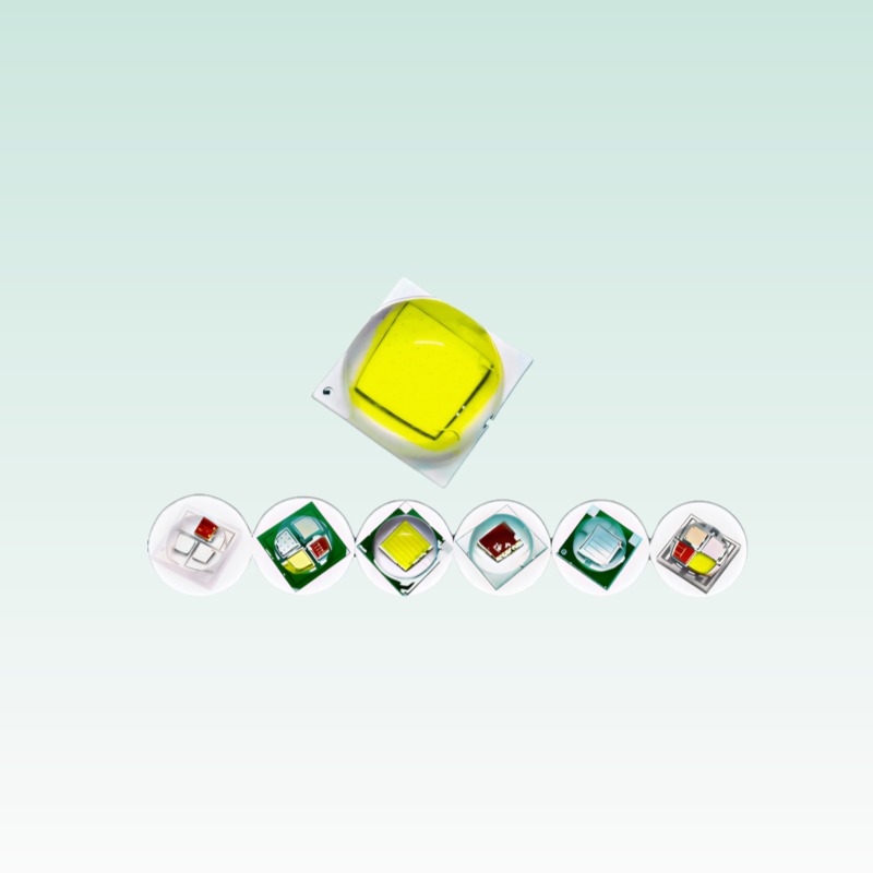









Application Note | AN-001
Thermal Management Design Guide for LED Applications
Published: September 2026 | Category: Application Notes | Keywords: LED thermal management, junction temperature, heat sink design, thermal resistance, LED cooling
1. Introduction
Thermal management is the single most critical factor in LED product design. Unlike incandescent sources that radiate heat as infrared energy, LEDs convert only 30-40% of electrical input into visible light while the remaining 60-70% becomes heat. This heat must be conducted away from the LED junction through the package, solder joint, PCB, and heat sink. Failure to manage junction temperature (Tj) leads to reduced luminous flux, color shift, shortened lifetime, and catastrophic failure. This application note provides engineers with quantitative thermal design methodology, material selection criteria, and validation testing procedures for LED-based products.
2. Understanding LED Thermal Resistance
The thermal path from LED junction to ambient follows a series of thermal resistances, each representing a material interface or layer:
Thermal Resistance Stack-up (Rth j-a)
Rth(j-a) = Rth(j-s) + Rth(s-b) + Rth(b-c) + Rth(c-a)
Where:
– Rth(j-s): Junction to solder point (LED package internal)
– Rth(s-b): Solder point to board (solder joint + pad)
– Rth(b-c): Board to case (PCB thermal conductivity)
– Rth(c-a): Case to ambient (heat sink + convection)
2.1 Junction-to-Solder Point Resistance (Rth j-s)
This is specified in LED datasheets and varies significantly by package type. Lower Rth(j-s) values indicate better internal thermal design:
| LED Package | Typical Rth(j-s) | Max Junction Temp | Power Dissipation |
|---|---|---|---|
| SMD 2835 | 15-25 C/W | 125C | 0.2-0.5W |
| SMD 3030 | 10-18 C/W | 125C | 0.5-1.0W |
| SMD 3535 | 6-12 C/W | 150C | 1.0-3.0W |
| SMD 5050 | 8-15 C/W | 125C | 0.5-1.5W |
| High-Power (Luxeon/Cree) | 2-8 C/W | 150C | 3.0-10W |
| COB LED | 1-5 C/W | 150C | 10-100W |
2.2 PCB Thermal Considerations
The PCB is the first major thermal bottleneck after the LED package. Standard FR-4 has a thermal conductivity of only 0.3 W/mK, which is inadequate for power LEDs. The following PCB substrates are recommended for different power levels:
| PCB Type | Thermal Conductivity | Recommended Power | Cost Factor |
|---|---|---|---|
| FR-4 Standard | 0.3 W/mK | < 0.5W per LED | 1x |
| FR-4 with thermal vias | 1.5-3.0 W/mK (effective) | 0.5-1.5W per LED | 1.5x |
| MCPCB (Aluminum) | 1.0-2.0 W/mK | 1.0-5.0W per LED | 2-3x |
| MCPCB (High-k) | 2.0-4.0 W/mK | 3.0-10W per LED | 3-4x |
| Ceramic (Al2O3) | 20-30 W/mK | 5.0-20W per LED | 5-8x |
| Ceramic (AlN) | 150-180 W/mK | 10-50W per LED | 8-12x |
3. Heat Sink Design Methodology
Heat sink selection follows a systematic thermal budget approach. The designer allocates the available temperature drop (Tj_max – T_ambient) across each thermal resistance in the path, then selects materials and geometries to meet each budget.
3.1 Thermal Budget Calculation
Example Calculation
Given:
– LED: SMD 3030, 1W input power, Rth(j-s) = 12 C/W
– Max junction temperature: 125C
– Ambient temperature: 40C (worst case)
– PCB: MCPCB, Rth(s-b) = 2 C/W, Rth(b-c) = 1 C/W
– Target: Tj < 100C (derated for 50,000h lifetime)
Required Rth(c-a) = (Tj_max – T_ambient) / P – Rth(j-s) – Rth(s-b) – Rth(b-c)
Rth(c-a) = (100 – 40) / 1 – 12 – 2 – 1 = 60 – 15 = 45 C/W
A heat sink with Rth < 45 C/W is required. This is achievable with a moderate aluminum extrusion heat sink with fin area of approximately 20 cm2.
3.2 Heat Sink Material Selection
Aluminum alloy 6063-T5 is the industry standard for LED heat sinks due to its excellent thermal conductivity (200 W/mK), formability for extrusion, and corrosion resistance. Copper offers 50% higher conductivity but at 3x cost and 3x weight. For weight-sensitive applications, graphite composite heat sinks provide 1.5x conductivity of aluminum at 60% weight.
3.3 Heat Sink Geometry Optimization
Heat sink performance depends on fin spacing, fin height, and base thickness. Optimal fin spacing balances surface area against airflow restriction. For natural convection, fin spacing of 6-10mm is optimal. For forced air (fan), 3-5mm spacing allows more fins in the same volume. Fin height should be at least 3x the fin gap to maximize surface area utilization.
4. Thermal Interface Materials (TIM)
The interface between PCB and heat sink introduces additional thermal resistance that is often overlooked. Air gaps of even 0.1mm can add 10-20 C/W of thermal resistance due to air’s poor conductivity (0.026 W/mK). Thermal interface materials fill these gaps:
| TIM Type | Conductivity (W/mK) | Application | Typical Rth |
|---|---|---|---|
| Thermal Grease | 0.5-3.0 | Thin bond line | 0.2-0.5 C/W |
| Thermal Pad | 1.0-6.0 | Gap filling | 0.5-2.0 C/W |
| Phase Change | 0.5-4.0 | Reflow compatible | 0.3-0.8 C/W |
| Solder (SAC305) | 55 | Direct attach | 0.05-0.1 C/W |
5. Active Cooling Solutions
For high-density LED arrays (>50W total power), passive cooling may be insufficient. Active cooling solutions include:
- Axial Fans: DC brushless fans (40-120mm) provide 10-100 CFM airflow. Suitable for LED panels, grow lights, and high-bay fixtures. Add 2-5 C/W improvement over passive.
- Blowers (Centrifugal): Better for compact enclosures with restricted airflow paths. Common in LED projectors and automotive headlights.
- Heat Pipes: Two-phase heat transfer devices with effective conductivity of 10,000+ W/mK. Ideal for space-constrained applications like LED spotlights and downlights.
- Vapor Chambers: Flat heat pipes covering large areas. Used in high-power LED flood lights (100W+) and stadium lighting.
- Liquid Cooling: Microchannel cold plates with water/glycol coolant. Reserved for extreme density applications (>500W) such as LED laser replacement and stage lighting.
6. Thermal Validation Testing
Thermal design must be validated through measurement. The following methods are industry standard:
6.1 Junction Temperature Measurement
Direct junction temperature measurement uses the LED’s own forward voltage (Vf) as a temperature sensor. The Vf-Tj relationship is calibrated in a temperature-controlled oven: drive the LED with a low sense current (e.g., 10mA), measure Vf at multiple temperatures, and establish the K-factor (dVf/dT, typically -1.5 to -2.5 mV/C). In operation, rapidly switch between drive current and sense current to measure Vf, then calculate Tj = T_ref + (Vf_measured – Vf_ref) / K-factor.
6.2 IR Thermography
Infrared thermal imaging cameras provide surface temperature maps of the PCB, heat sink, and fixture housing. This identifies hot spots, verifies heat distribution uniformity, and detects thermal bottlenecks. For accurate LED surface measurement, the LED lens must be painted with a thin layer of matte black paint (emissivity ~0.95) to avoid reflective IR measurement errors.
6.3 Compliance Standards
- JEDEC JESD51-50: Thermal resistance measurement of LEDs
- IEC 60598-1: Luminaire thermal safety (touch temperature limits)
- MIL-STD-883: Thermal shock and cycling for LED packages
- LM-80 (IESNA): Lumen maintenance testing at elevated temperatures
7. Design Checklist
- [ ] LED datasheet Rth(j-s) value obtained and verified
- [ ] Maximum junction temperature defined (recommend < 100C for 50,000h L70)
- [ ] Worst-case ambient temperature determined (including enclosed fixture rise)
- [ ] Thermal budget calculated and allocated across all interfaces
- [ ] PCB substrate selected appropriate for power density
- [ ] Thermal interface material selected and gap specified
- [ ] Heat sink Rth calculated and verified with supplier data
- [ ] Junction temperature validated by measurement or simulation
- [ ] Touch temperature verified < 60C (IEC 60598 accessible surfaces)
- [ ] Thermal cycling test (-40C to +85C, 200 cycles) passed
8. Thermal Design Case Studies (Illustrative Examples)
8.1 Case Study: 1 W High-Power LED (3535 Package) in an Outdoor Floodlight
A single 3535 high-power LED is operated at IF = 350 mA with a forward voltage of approximately 2.9 V, giving a power dissipation of 1.0 W. The datasheet specifies a junction-to-solder-point thermal resistance Rth j-s of 6 °C/W. The luminaire is an outdoor floodlight that must operate in a summer ambient of 40 °C, and the design target is a junction temperature no higher than 105 °C, which preserves a 20 °C engineering margin below the 125 °C absolute maximum rating.
The available thermal budget is therefore 105 − 40 = 65 °C. The total junction-to-ambient resistance must satisfy Rth j-a of 65 °C/W or less. Breaking the path into its physical segments: the solder point to MCPCB contribution (100 µm dielectric, approximately 25 mm² thermal pad with 1 W/m·K dielectric conductivity) is around 4 °C/W; the thermal interface material (grease at 50 µm) adds roughly 2 °C/W. This leaves 65 − (6 + 4 + 2) = 53 °C/W available for the heat sink itself.
A compact extruded aluminum heat sink of 80 × 60 × 40 mm with twelve fins provides a natural-convection resistance of approximately 6 °C/W — nearly nine times better than required. Even with realistic degradation factors, such as dust fouling increasing sink resistance by 50 percent and enclosure air recirculation raising the local ambient by 10 °C, the junction temperature remains Tj = 50 + 1.0 × (6 + 4 + 2 + 9) = 71 °C, comfortably below target. This margin is intentional: it absorbs component tolerances, assembly variation, and end-of-life dust accumulation.
To validate this budget, apply the measurement methods in Section 6 of this note: bond a 36-gauge thermocouple to the solder pad and read the steady-state temperature in a 40 °C chamber. A reading of Tsp = 63 °C, for example, gives Tj = Tsp + P × Rth j-s = 63 + 6 = 69 °C — within a few percent of the calculated value. The design can then be frozen with the documented via pattern, TIM type, and mounting torque specification.
8.2 Case Study: 2835 SMD LED Strip on FR4
A linear module carries 96 pieces of 2835 SMD LEDs, each dissipating 0.2 W at 60 mA, for a total of 19.2 W distributed along a 1000 × 15 mm FR4 strip with 2 oz copper. FR4 has a through-plane conductivity of only about 0.3 W/m·K, which makes the board itself a poor conductor; the design strategy is to spread heat laterally in the copper and export it into the mounting surface.
Because drilled via arrays are impractical on a flexible or adhesive-mounted strip, the strip is bonded into an aluminum channel with thermal tape of 0.6 W/m·K at 100 µm. For the full strip footprint this interface contributes roughly 2.5 °C/W to the channel. In a prototype measurement at full power, a construction like this shows a pad-to-channel rise on the order of 14 °C and a channel-to-ambient rise of 15 °C in still air. The junction temperature is then Tj = 25 + 15 + 14 + 0.2 × 12 ≈ 56 °C, where 12 °C/W is the 2835 junction-to-pad resistance.
The lesson from this case is that in strip-type products the mechanical mounting is the heat sink. The FR4 contributes spreading, not conduction to ambient. Designers who validate a strip lying on a bench without its channel routinely under-predict junction temperature by more than 30 °C.
9. Common Thermal Design Mistakes
The following table summarizes the failure patterns our applications team encounters most frequently during customer design reviews, together with their consequences and the corrective actions we recommend.
| Mistake | Typical Consequence | Prevention |
|---|---|---|
| Too few thermal vias under LED thermal pads | Local hot spot, accelerated lumen depreciation | Use 4 or more filled 0.3 mm vias per pad, or move to MCPCB above roughly 0.35 W per LED |
| TIM applied too thick or with voids above 25% | 5 to 15 °C of avoidable junction rise | Controlled deposit or stencil printing; verify by acoustic or X-ray inspection on pilot units |
| Sealed IP65 enclosure with no conduction path | Internal ambient trapped 20 to 30 °C above outside air | Bond the LED board to the housing so the enclosure itself becomes the heat sink |
| Ignoring altitude derating above 2,000 m | Natural convection capability drops 10 to 20% | Apply the heat sink manufacturer’s altitude correction factor |
| Placing current-setting resistor next to the LED | Radiant heating of the phosphor layer | Move power resistors off the LED board or use a constant-current driver |
| Reusing a validated design at a higher drive current | Junction temperature rises with power, not with expectations | Re-run the thermal budget and re-validate Tsp whenever power changes |
| Skipping temperature verification on pilot builds | Field failures discovered by customers | Always instrument the first article build before releasing to production |
10. Frequently Asked Questions
What is the maximum allowable junction temperature for Queendom LEDs?
Check the absolute maximum rating in each product datasheet — 110 to 125 °C is typical by package family — and for long-life applications keep continuous junction temperature at or below 85 °C. Field experience links every 10 °C reduction in junction temperature to a roughly two-fold improvement in lumen maintenance life.
Can standard FR4 handle a 0.5 W LED?
It is marginal. At 0.5 W per device you should either provide a dense via farm with 2 oz or heavier copper, or move to a metal-core board. Between 0.2 and 0.35 W, FR4 with good copper spreading is generally acceptable; verify with a pad measurement on the first prototype.
How critical is thermal interface material thickness?
Every 25 µm of excess grease at 1 W adds approximately 1 °C. The bigger risk is voids: a 30 percent void rate under a high-power pad can add 5 to 10 °C because heat is forced through the remaining contact area.
When is active cooling justified?
When the passive heat sink required to meet the thermal budget becomes larger, heavier, or more expensive than a fan. In practice this crossover occurs somewhere between 15 and 25 W of dense LED power in constrained enclosures. Remember that fans introduce a reliability component of their own — a two-year fan life can dominate an otherwise 50,000-hour LED system.
How can I estimate junction temperature without laboratory equipment?
Attach a fine-gauge thermocouple to the solder pad or the thermal pad of the package and read the steady-state temperature at full power. Then add P × Rth j-s from the datasheet. This two-component method is typically accurate to within a few degrees and is sufficient for design verification.
Does solder mask color or PCB finish matter?
Only marginally. Solder mask openings over thermal pads help by a degree or two, but the board stack-up, copper weight, and interface quality dominate the result. Do not spend engineering effort on mask optimization before the via and TIM design is settled.
Related Resources
Datasheets: LED Datasheet Center
Testing: LM-80 Test Reports
Selection: LED Package Selection Guide
Support: Contact Technical Sales
Need help with your LED thermal design?