
 English
 Afrikaans
 Albanian
 Amharic
 Arabic
 Armenian
 Azerbaijani
 Basque
 Belarusian
 Bengali
 Bosnian
 Bulgarian
 Catalan
 Cebuano
 Chichewa
 Corsican
 Croatian
 Czech
Czech Danish
 Dutch
Dutch Esperanto
 Estonian
 Filipino
 Finnish
 French
 Frisian
 Galician
 Georgian
 German
 Greek
Greek Gujarati
 Haitian Creole
 Hausa
Hausa Hawaiian
 Hebrew
 Hindi
Hindi Hmong
Hmong Hungarian
 Icelandic
 Igbo
Igbo Indonesian
 Irish
Irish Italian
 Japanese
 Javanese
 Kannada
 Kazakh
 Khmer
Khmer Korean
 Kurdish (Kurmanji)
 Kyrgyz
 Lao
Lao Latin
Latin Latvian
 Lithuanian
 Luxembourgish
 Macedonian
 Malagasy
 Malay
Malay Malayalam
 Maltese
 Maori
Maori Marathi
 Mongolian
 Myanmar (Burmese)
 Nepali
 Norwegian
 Pashto
 Persian
 Polish
 Portuguese
 Punjabi
 Romanian
 Russian
 Samoan
 Scottish Gaelic
 Serbian
 Sesotho
 Shona
Shona Sindhi
 Sinhala
 Slovak
 Slovenian
 Somali
 Spanish
 Sudanese
 Swahili
 Swedish
 Tajik
Tajik Tamil
Tamil Telugu
 Thai
Thai Turkish
 Ukrainian
 Urdu
Urdu Uzbek
Uzbek Vietnamese
 Welsh
Welsh Xhosa
Xhosa Yiddish
 Yoruba
 Zulu
Zulu
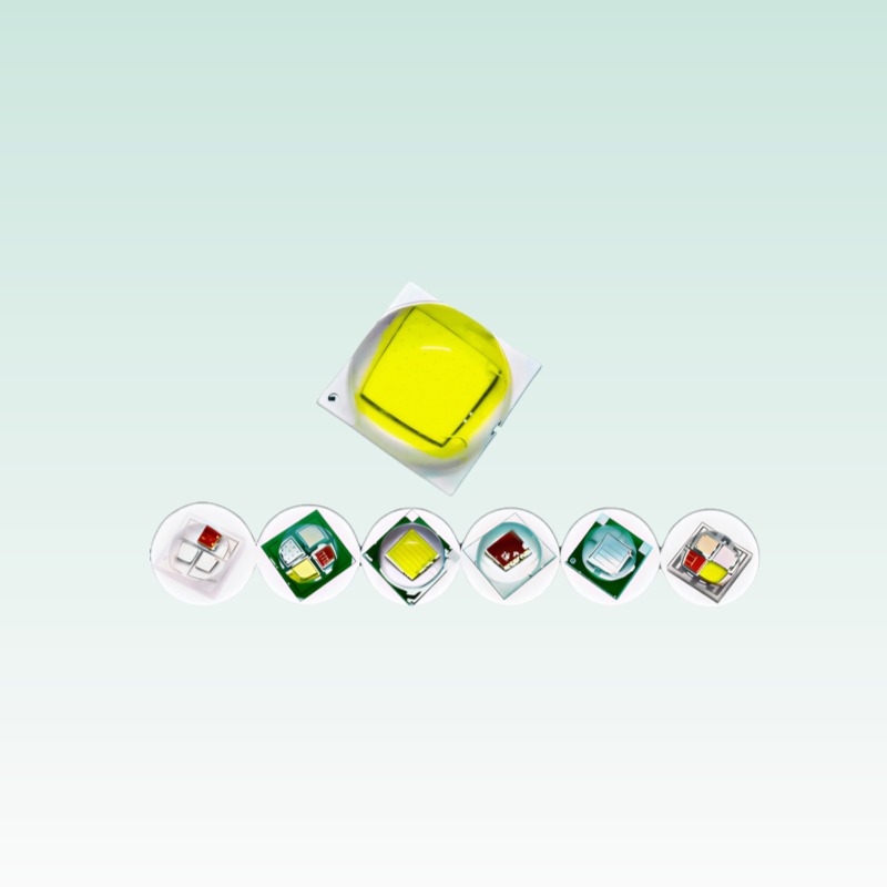
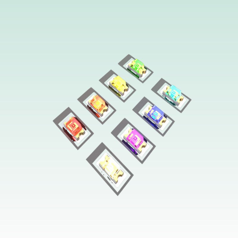
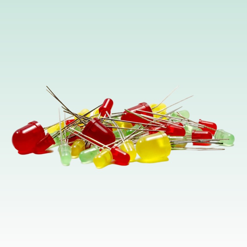
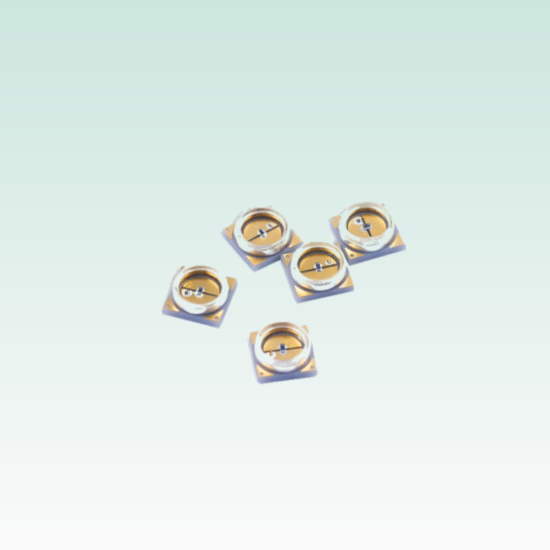
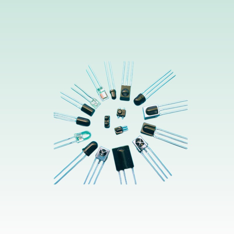
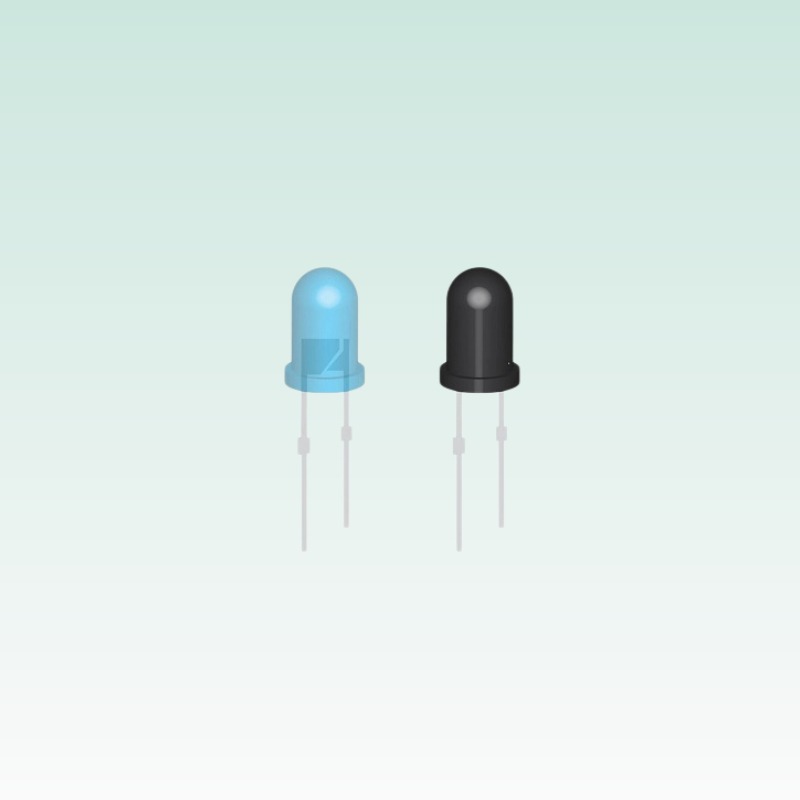





High-Power LED Failure Analysis
Ceramic high-power LED troubleshooting (1W–30W) — thermal fatigue, wire bond lift-off, phosphor degradation, and root-cause analysis based on LM-80/TM-21 test data and industrial field experience.
1. Overview of High-Power LED Failure Modes
High-power LEDs (1 W to 30 W, typically packaged on ceramic substrates with flip-chip or wire-bonded dies) operate at significantly higher current densities and junction temperatures than low-power SMD or DIP devices. This makes thermal and mechanical failure modes far more critical. Queendom ceramic high-power LEDs are designed for Tj up to 125 °C, but sustained operation near the maximum rating accelerates several degradation mechanisms.
Failure modes in high-power LEDs fall into five major categories:
- Thermal fatigue — solder layer delamination, die attach degradation, and package cracking from thermal cycling.
- Wire bond and interconnect failure — gold wire lift-off, heel cracking, and electrode corrosion.
- Chip-level degradation — dislocation climb, defect generation in the active region, and current crowding.
- Phosphor and encapsulant degradation — silicone yellowing, phosphor quenching, and delamination at the phosphor–silicone interface.
- Electrical overstress (EOS/ESD) — reverse bias breakdown, latch-up, and catastrophic forward surge.
2. High-Power LED Package Comparison Matrix
High-power LEDs are available in several ceramic package formats, each with different power handling, thermal characteristics, and failure-mode profiles. Understanding these differences is essential for accurate failure analysis and appropriate corrective action.
| Parameter | 3535 Ceramic | 5050 Ceramic | 7070 Ceramic | COB Array |
|---|---|---|---|---|
| Footprint (mm) | 3.5 × 3.5 | 5.0 × 5.0 | 7.0 × 7.0 | 10–50 mm dia. |
| Package Height | 1.2–1.5 mm | 1.4–1.8 mm | 1.8–2.3 mm | 1.5–3.0 mm |
| Power Range | 1–5 W | 3–20 W | 5–30 W | 10–300 W |
| Typical Drive Current | 350–1500 mA | 1–6 A | 2–10 A | 0.5–10 A (total) |
| Thermal Resistance θjc | 4–8 °C/W | 2–5 °C/W | 1–3 °C/W | 0.5–2 °C/W |
| Substrate Material | AlN / Al2O3 | AlN / Al2O3 | AlN (high k) | AlN / MCPCB |
| Die Attachment | AuSn eutectic | AuSn / Ag sinter | Ag sintered | Ag sinter / flip-chip |
| Interconnect Type | Gold wire bond | Gold wire / flip-chip | Flip-chip / Au wire | Flip-chip + gold wire |
| Primary Failure Mode | Wire bond lift-off | Die-attach delamination | Phosphor thermal quenching | Phosphor degradation |
| ESD Rating (HBM) | Class 2 (2 kV) | Class 2 (2 kV) | Class 3B (8 kV) | Class 3A/B |
| Typical Applications | Flashlights, IR emitters, UV curing | Automotive, horticulture, industrial curing | Stage lighting, high-bay, UV flood curing | Floodlights, stadium, COB modules |
Key takeaway for failure analysis: Smaller ceramic packages (3535, 5050) tend to fail by wire bond fatigue or die-attach delamination because of the higher thermal resistance per watt. Larger 7070 and COB packages, with better thermal paths, more often show phosphor and encapsulant degradation as the dominant wear-out mechanism, simply because they run at higher absolute flux densities at the phosphor layer.
3. Thermal Fatigue and Die-Attach Degradation
3.1 Solder Layer Delamination
Ceramic high-power LEDs use a gold-tin (AuSn) eutectic solder or silver sintered die-attach layer between the LED die and the ceramic submount. Repeated thermal cycling (e.g., –40 °C ↔ +125 °C per JEDEC JESD22-A104) causes fatigue crack propagation at the solder–die or solder–ceramic interface. Each cycle adds micro-cracks that progressively reduce the effective heat-dissipation area, raising thermal resistance θjc and accelerating lumen depreciation.
Symptoms: Gradual increase in forward voltage (Vf) at constant current, elevated case temperature, accelerated lumen decay (faster than TM-21 projection).
Root-cause verification: Use scanning acoustic microscopy (SAM) or cross-sectional SEM to image the die-attach layer. Delamination exceeding 20% of the die area is generally considered a failure criterion.
3.2 Thermal Resistance Drift
Thermal resistance θjc (junction-to-case) for a healthy Queendom 5050 high-power LED is typically 2–4 °C/W for single-die and 2–4 °C/W per die for multi-die COB. A drift of more than 20% above initial value indicates die-attach or package degradation and warrants failure analysis.
3.3 Ceramic Substrate Cracking
Alumina (Al₂O₃) and aluminum nitride (AlN) ceramic substrates are mechanically rigid but brittle. Mechanical shock, improper PCB mounting (uneven screw torque), or rapid thermal shock can cause substrate cracking. Cracked ceramics often show intermittent electrical contact or partial loss of thermal path.
4. Wire Bond and Interconnect Failures
4.1 Gold Wire Lift-Off
High-power LEDs with wire-bonded dies use 1.0–2.0 mil gold ball bonds. At high operating temperatures combined with vibration or thermal cycling, the bond heel can crack and eventually lift off. This is the most common field failure mode for 1–5 W discrete high-power LEDs.
Symptoms: Sudden open-circuit failure, intermittent operation, Vf jump when tapped.
Prevention: Queendom high-power products use robust ball-bond parameters optimized per JEDEC J-STD-001, with minimum bond shear strength exceeding MIL-STD-883 Method 2019 requirements.
4.2 Flip-Chip Solder Joint Fatigue
Flip-chip high-power LEDs (common in COB and high-density arrays) use solder bumps for both electrical and thermal connection. Thermal cycling causes fatigue in the solder bumps, particularly at the die-side intermetallic compound (IMC) layer. Kirkendall voiding at the Au–Sn IMC interface is a known long-term failure mechanism.
5. Chip-Level Degradation
5.1 Dislocation Climb and Dark-Spot Defects
At high current densities (> 35 A/cm²) and elevated junction temperatures, threading dislocations in the GaN epitaxial layer can climb and propagate, forming non-radiative recombination centers known as “dark line defects” (DLDs) or “dark spot defects” (DSDs). This manifests as localized dark regions visible under electroluminescence imaging and a corresponding drop in luminous flux.
5.2 Current Crowding
Poor current spreading due to degraded transparent conductive oxide (TCO) layers or non-uniform p-type contact can cause current crowding at the die edges or p-pad periphery, accelerating local degradation and creating thermal hotspots.
6. Phosphor and Encapsulant Degradation
6.1 Silicone Yellowing
High-power white LEDs use silicone encapsulant loaded with YAG:Ce phosphor. At sustained junction temperatures above 100 °C and high blue-photon flux, the silicone matrix undergoes photo-thermal oxidation, gradually yellowing and shifting the color point toward warmer CCT. High CRI (Ra 90+) formulations with additional red nitride phosphors are particularly susceptible to temperature-induced spectral shift.
6.2 Phosphor Thermal Quenching
Phosphor conversion efficiency decreases with temperature (thermal quenching). For YAG:Ce, quenching is typically <10% at 125 °C, but for some nitride red phosphors it can exceed 20%. This causes both a lumen drop and a CCT shift. Proper thermal design keeps the phosphor temperature well below the quenching threshold.
6.3 Phosphor–Silicone Delamination
At the interface between the phosphor-loaded silicone and the LED die surface, CTE (coefficient of thermal expansion) mismatch can cause delamination after repeated thermal cycling. Delaminated regions show as dark spots in near-field optical imaging.
7. Electrical Overstress (EOS) and ESD
High-power LEDs have larger die sizes than SMD LEDs, which generally gives them better ESD withstand capability (typically Class 2 per ANSI/ESDA/JEDEC JS-001, i.e., ≥ 2 kV HBM). However, they are still vulnerable to:
- Forward surge — inrush current during hot-plug or power-supply transient can melt bond wires or damage the active region.
- Reverse over-voltage — electrostatic discharge or inductive kickback can cause immediate reverse breakdown.
- Latch-up — in some multi-junction structures, localized thermal runaway can create a low-resistance path.
8. Case Study: 50W COB LED Failure in Stadium Lighting
Application: Outdoor stadium floodlight using 50 W COB LED modules.
Failure symptom: 15% of units showed >30% lumen depreciation after 6,000 hours, with a noticeable shift to warmer CCT.
Investigation:
- Thermal imaging revealed hotspot temperatures 25 °C above design target.
- Cross-sectional analysis showed die-attach solder delamination of 35–40%.
- FTIR analysis confirmed silicone encapsulant oxidation (carbonyl peak formation).
- Root cause: insufficient thermal interface material (TIM) application during module assembly, combined with an under-sized heat sink.
Corrective action: Revised TIM application process with automated dispense, upgraded heat sink from 2.0 °C/W to 1.2 °C/W, and added 100% thermal resistance screening at final test. Field return rate dropped below 1% after the fix.
9. Prevention Strategies and Selection Guidelines
9.1 Proper Thermal Design
Design the thermal path so that Tj stays below 85 °C at maximum rated current for long-life applications. Use Queendom’s thermal resistance data (θjc, θsp) to calculate required heat sink size.
9.2 Drive Current De-rating
For high-reliability applications (outdoor lighting, industrial, horticulture), de-rate the drive current to 70–80% of the maximum rated current. Every 10 °C reduction in Tj roughly doubles the time to 70% lumen maintenance (L70).
9.3 ESD Protection in Production
Follow ANSI/ESD S20.20 ESD control program requirements. High-power LEDs should be handled only at grounded workstations with proper wrist straps and ionizers.
9.4 Solder Reflow Profile Control
Follow Queendom’s recommended reflow profile (peak 260 °C, < 30 s above 250 °C per J-STD-020). Excessive peak temperature or time above liquidus causes AuSn solder migration and IMC overgrowth.
10. FAQ
Q: What is the typical L70 lifetime of Queendom high-power LEDs?
A: At Tj = 85 °C and rated current, Queendom ceramic high-power LEDs deliver > 50,000 hours to L70 per LM-80 / TM-21 projection. Actual lifetime depends on drive current, thermal management, and environmental conditions.
Q: Can a single failed LED be replaced on a COB array?
A: No, COB (chip-on-board) LEDs are monolithic arrays. If one die fails catastrophically (short), the entire COB may need replacement. For high-availability applications, use drivers with open/short circuit protection.
Q: How do I distinguish between thermal degradation and phosphor degradation?
A: Measure both luminous flux and CCT shift. If flux drops but CCT remains stable, it is likely chip-level or die-attach thermal degradation. If flux drops AND CCT shifts warmer (or CRI drops), phosphor/encapsulant degradation is likely.
11. Related Resources
- Thermal Management Design Guide for LED Applications
- LM-80 Testing and LED Lifetime Estimation
- High-Power LED Datasheets
- ESD Damage and Prevention
- Industrial LED Reliability White Paper
- SMD LED Package Selection Guide (2835 / 3030 / 3535 / 5050)
Need a failure analysis report for your application?
Contact our application engineering team at support@queendomlamp.com with your failure sample details. We provide root-cause analysis, FA reports, and corrective action recommendations for Queendom high-power LED products.