

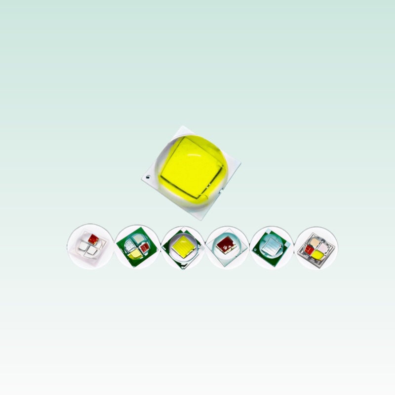
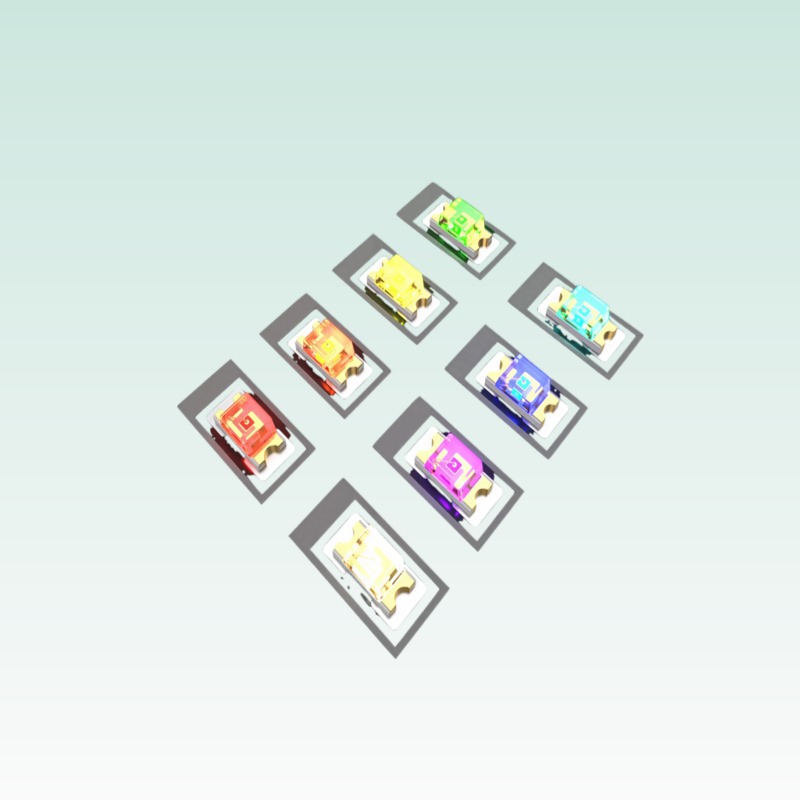
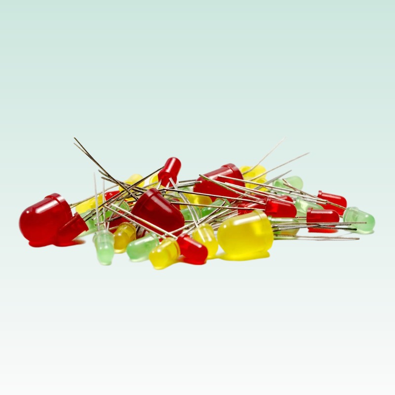
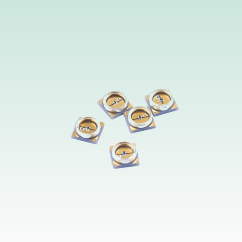
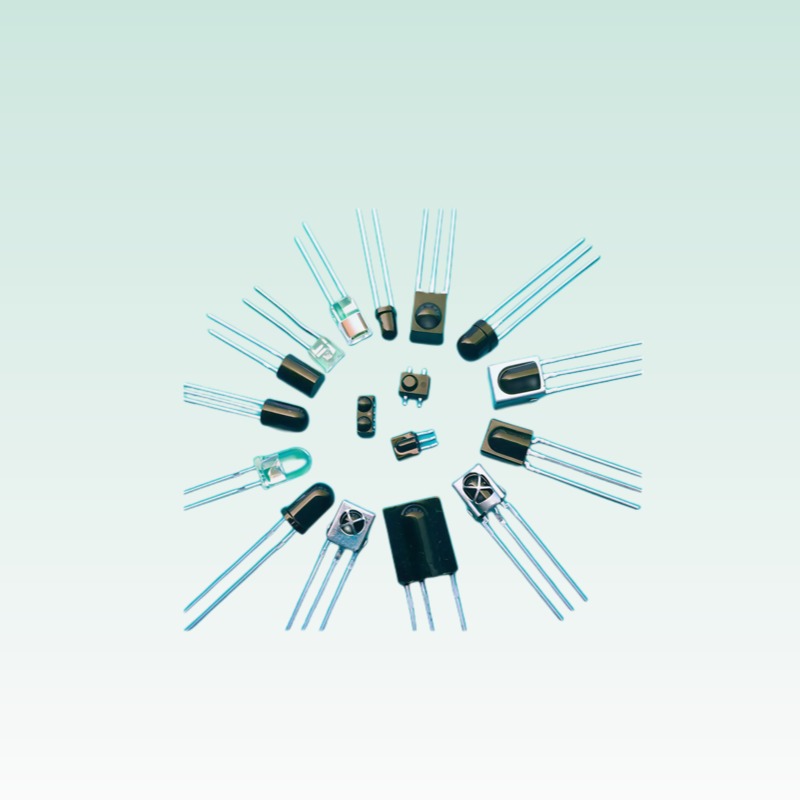
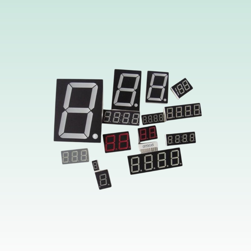
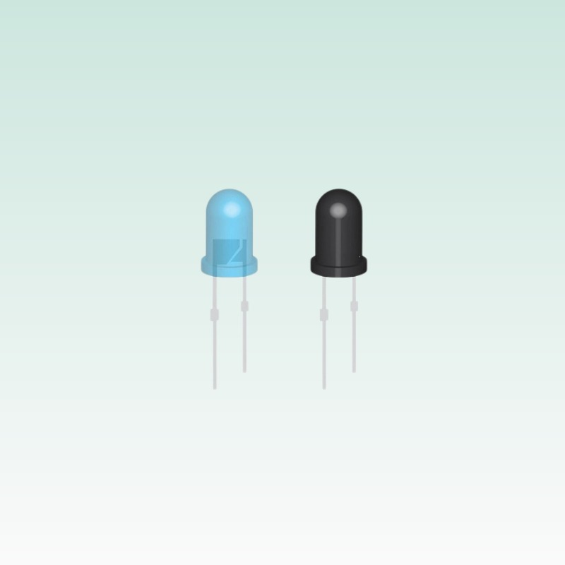
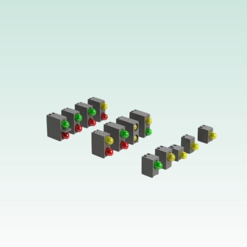






Multi-colour LED systems have moved from decorative accents into architectural facades, automotive interior ambience, signage, appliance indicators and entertainment displays. The engineering has changed with them: what used to be a question of “which colour” is now a question of colour gamut, dimming linearity, data timing, thermal derating across three or four junctions in one package, and colour consistency over thousands of units. This white paper is written for product and lighting engineers specifying Addressable RGB and multi-colour SMD emitters, and it sets out the four variables that determine system quality. QUEENDOM’s J-16 0807 Addressable RGB, J-17 3528 multi-color, J-18 3535 multi-color and J-19 5050 multi-color families are used throughout as the worked examples.
One terminology note before proceeding. The correct English term for these devices is Addressable RGB, or multi-colour SMD, depending on whether they contain integrated control silicon. Literal translations of the Chinese trade term are not used in English-language technical documentation and should not appear in specifications, datasheets or platform listings.
1. What “addressable” means, and why it changes the design
A conventional multi-colour LED is a three- or four-junction package with separate anode or cathode connections per colour. The designer selects the colour by driving each channel with a different current. An Addressable RGB device contains an integrated control circuit inside the package. Each device has a data input and a data output; devices are chained, and each device reads the first bits of the incoming stream, keeps those addressed to itself, and forwards the remainder. This reduces the wiring from three or four power channels per colour position to a single serial data line plus power and ground.
The trade-off is that the design problem shifts from analog current control to digital protocol integrity.
| Attribute | Conventional multi-colour SMD | Addressable RGB |
|---|---|---|
| Control interface | Separate channel per colour | Single serial data line |
| Wiring per pixel position | 4–5 conductors | 3 conductors (VDD, DIN/DOUT, GND) |
| Per-pixel addressing | Requires external driver per channel | Built into the package |
| Colour resolution | Limited by driver DAC | Typically 8 bit per colour, 16.7 M colours |
| Data rate limiting factor | Driver bandwidth | Protocol timing and cable capacitance |
| Failure mode | One channel lost | Downstream chain may stop forwarding |
| Best fit | Small counts, high flux per position | Large pixel counts, fine granularity |
The addressable architecture makes 1,000-pixel installations practical where a conventional approach would require 3,000 to 4,000 individual drive channels. It also introduces a new critical failure mode: because data is passed along the chain, a single device that fails to forward data blanks everything downstream of it.
2. Colour coordinates and gamut planning
Colour specification starts with the CIE 1931 chromaticity diagram. Each emitter’s colour is a point within the diagram; three emitters form a triangle, and that triangle is the gamut the system can reproduce. The larger the triangle, the more saturated colours are available — but a large triangle also means that reproducing white requires careful balancing.
2.1 Typical primary coordinates
The table below gives representative CIE 1931 coordinates for the primaries used in the J-16 to J-19 families. Exact coordinates are bin-dependent and must be confirmed per production lot for colour-critical applications.
| Colour | Dominant wavelength | CIE x | CIE y | Package availability |
|---|---|---|---|---|
| Red | 620–625 nm | 0.70 | 0.30 | J-16, J-17, J-18, J-19 |
| Green | 520–530 nm | 0.17 | 0.72 | J-16, J-17, J-18, J-19 |
| Blue | 465–470 nm | 0.13 | 0.06 | J-16, J-17, J-18, J-19 |
| White (mixed) | — | 0.31 | 0.33 | J-18, J-19 (RGBW variants) |
| Amber / yellow | 590 nm | 0.57 | 0.42 | J-17, J-18, J-19 |
| Cyan (multi-colour) | 505 nm | 0.05 | 0.50 | J-18, J-19 |
2.2 Gamut coverage
Gamut coverage is the fraction of a reference colour space that a system can reproduce. Multi-colour SMD systems with narrow-band primaries typically cover a large fraction of the sRGB or Rec. 2020 triangle, and the limiting factor is usually the green primary rather than red or blue.
| Reference space | Typical coverage with J-16 primary set | Limiting primary |
|---|---|---|
| sRGB | 95–100 % | Blue (short-wavelength limit) |
| Adobe RGB | 85–95 % | Green |
| DCI-P3 | 88–96 % | Green |
| Rec. 2020 | 65–80 % | Green (needs narrower spectrum) |
3. PWM dimming and its linearity
Colour and brightness are almost always controlled by pulse-width modulation. The LED is driven at a fixed forward current and the duty cycle is varied. Two properties matter for system quality: the linearity of perceived output against duty cycle, and the modulation frequency relative to camera and human perception.
| Dimming parameter | Typical specification | Consequence if inadequate |
|---|---|---|
| PWM frequency | ≥ 1 kHz (flicker-free), 3–20 kHz common | Visible flicker; camera banding |
| Minimum duty cycle | 0.1–1 % | Cannot dim to true black; colour shift at low levels |
| Duty resolution | 8 bit (256 steps) or 12–16 bit | Visible steps in fades |
| Rise/fall time | < 1 µs | Non-linearity at low duty cycle |
| Current matching across channels | ±5 % | Colour shift during dimming |
| Thermal coefficient of output | -0.2 to -0.5 %/K | Colour drift as the fixture warms |
The most common non-linearity arises at low duty cycles, where the driver’s finite rise and fall times consume a significant fraction of the pulse. If the rise time is 1 µs and the pulse width is 5 µs, the emitter spends a measurable share of its on-time in a transition region, and the output at 1 % duty is not 1 % of the full-duty output.
3.1 Perceived brightness and gamma
PWM duty cycle is linear in light output but not in perceived brightness. Human brightness perception follows approximately a power law, so a linear duty ramp looks as though it stalls at the bright end and rushes at the dark end. Controllers therefore apply a gamma correction, typically γ ≈ 2.2 to 2.8, mapping the 8-bit control value to duty cycle.
| Control value (8 bit) | Duty, linear map | Duty, γ = 2.2 map | Perceived result |
|---|---|---|---|
| 0 | 0 % | 0 % | Off |
| 32 | 12.5 % | 0.7 % | Very dim, smooth |
| 64 | 25.0 % | 3.9 % | Planos acotados para integración mecánica. |
| 128 | 50.0 % | 21.8 % | Medium |
| 192 | 75.0 % | 53.0 % | Bright |
| 255 | 100 % | 100 % | Garantía completa |
Without gamma correction, an 8-bit fade appears to have approximately five visible steps rather than the 256 the data format implies.
4. Data protocol and timing
Addressable RGB devices are driven by a serial protocol in which a logic-1 and a logic-0 are distinguished by pulse width rather than by level. The controller emits a reset or latch period to terminate a frame and begin the next. Timing margins are tight and cable capacitance is the usual cause of failure in large installations.
Protocol families differ in their exact timings and in bit order, and one family’s waveform will not drive another family’s device. The table below gives representative values for the two most widely encountered families.
| Timing parameter | Family A (800 kHz class) | Family B (800 kHz class, alternate) |
|---|---|---|
| Data rate | 800 kbit/s | 800 kbit/s |
| Logic 0 high time | 0.30 ± 0.15 µs | 0.35 ± 0.15 µs |
| Logic 0 low time | 0.90 ± 0.15 µs | 0.80 ± 0.15 µs |
| Logic 1 high time | 0.60 ± 0.15 µs | 0.70 ± 0.15 µs |
| Logic 1 low time | 0.60 ± 0.15 µs | 0.60 ± 0.15 µs |
| Reset / latch low | > 50 µs | > 50 µs |
| Bit order | GRB, MSB first | RGB or GRB, MSB first |
| Bits per pixel | 24 (8 per colour) | 24 (8 per colour) |
| Refresh rate at 1,024 pixels | ≈ 32 Hz | ≈ 32 Hz |
Two practical consequences follow. First, at 800 kbit/s the maximum refresh rate falls as pixel count rises: 1,024 pixels at 24 bits each is 24,576 bits, or about 31 ms per frame, which is roughly 32 Hz. Above several thousand pixels the installer must either accept visible refresh artefacts or segment the chain and drive it in parallel. Second, cable capacitance limits the distance between devices; a long run of thin cable rounds the pulse edges until logic 0 and logic 1 become indistinguishable. The maximum reliable spacing is typically 0.5 to 2 m between devices for a well-matched wiring scheme, and it must be verified rather than assumed.
5. Product mapping
The four families are chosen by package size, flux and whether integrated control silicon is present.
| Requirement | Recommended part | Package | Characteristic | Control interface |
|---|---|---|---|---|
| Fine-pitch pixel strip | J-16 0807 Addressable RGB | 0.8 × 0.7 mm | Integrated control, chained data | Serial data, 3-wire |
| Indicator and backlight | J-17 3528 multi-color | 3.5 × 2.8 mm | Standard SMD, per-colour anodes | Analog, 4-wire |
| Architectural point source | J-18 3535 multi-color | 3.5 × 3.5 mm | Ceramic body, RGB and RGBW variants | Analog or addressable variant |
| High-flux effects and signage | J-19 5050 multi-color | 5.0 × 5.0 mm | Highest flux per position | Analog or addressable variant |
| Parameter | J-16 0807 | J-17 3528 | J-18 3535 | J-19 5050 |
|---|---|---|---|---|
| Footprint | 0.8 × 0.7 mm | 3.5 × 2.8 mm | 3.5 × 3.5 mm | 5.0 × 5.0 mm |
| Channels | 3 (RGB) + control IC | 3 (RGB) | 3 or 4 (RGB / RGBW) | 3 or 4 (RGB / RGBW) |
| Typical luminous intensity per channel | 30–80 mcd | 60–180 mcd | 120–300 mcd | 300–800 mcd |
| Forward voltage, R / G / B | 2.0 / 2.9 / 2.9 V | 2.0 / 3.0 / 3.0 V | 2.1 / 3.1 / 3.1 V | 2.1 / 3.2 / 3.2 V |
| Drive current per channel | 5–20 mA | 20 mA | 20–60 mA | 20–100 mA |
| Viewing angle | 120° | 120° | 120° | 120° |
| Integrated control IC | Yes | No | Optional | Optional |
| Resistencia Térmica | ~350 K/W | ~180 K/W | ~60 K/W | ~35 K/W |
| Best mount | Flexible PCB | FR-4 | FR-4 or MCPCB | MCPCB above 60 mA/ch |
5.1 Thermal derating in multi-junction packages
A three-channel device dissipating 0.2 W has three junctions heating one package. When all three channels are at full drive, the package temperature rises faster than a single-colour device of the same total power would suggest, and each channel’s output falls accordingly. Because red, green and blue emitters have different temperature coefficients, the colour balance also shifts: red output typically falls faster with temperature than blue.
| Condition | Package temperature | Red relative output | Green relative output | Blue relative output | Colour shift |
|---|---|---|---|---|---|
| 25 °C, single channel | 30 °C | 100 % | 100 % | 100 % | Reference |
| 25 °C, all channels | 45 °C | 93 % | 96 % | 97 % | Slight red loss |
| 55 °C, all channels | 78 °C | 82 % | 89 % | 92 % | Noticeable red loss |
| 85 °C, all channels | 108 °C | 71 % | 81 % | 86 % | Strong red loss, warm shift |
The practical consequence is that white-point calibration performed on a cold fixture will not hold once the fixture reaches operating temperature, unless the controller applies per-channel temperature compensation.
6. Common mistakes and how to avoid them
| Mistake | Consequence | Correction |
|---|---|---|
| Mixing protocol families on one chain | Downstream devices dark or flickering | Confirm the protocol family for every device on the chain |
| PWM frequency below 1 kHz | Visible flicker and camera banding | Specify ≥ 1 kHz; 3 kHz or above for camera-adjacent work |
| No gamma correction | Fades appear to have five steps, not 256 | Apply γ ≈ 2.2 in the controller |
| Cold-state colour calibration | White point drifts warm when hot | Calibrate warm, or add per-channel temperature compensation |
| Long cable runs with thin conductors | Pulse rounding, intermittent pixel dropouts | Keep device spacing short; verify edges with a scope |
| Sizing the power supply at nominal current | Voltage sag at full white | Budget 120 % of maximum simultaneous current |
| Ignoring the propagation delay per pixel | Lower refresh rate than expected | Calculate chain length from the data rate |
| Describing the product as a literal translation of the trade term | Non-standard terminology in English materials | Use Addressable RGB or multi-colour SMD |
7. Verification and test methods
- Chromaticity and flux measurement — measure each primary on a calibrated spectroradiometer or colourimeter at rated current and at the production case temperature. Report CIE 1931 coordinates, dominant wavelength and flux per channel.
- Colour consistency across a batch — measure a sample across the production lot and report the distribution in u′v′ space. Multi-colour systems without a binning statement show visible variation between adjacent units.
- PWM linearity and flicker — measure light output at 10 duty values from 0.5 % to 100 % and plot against duty. Confirm the achievable minimum duty and verify the flicker index at the specified PWM frequency.
- Protocol timing verification — capture the data waveform at the first and last device in a full-length chain at the maximum specified cable length, and confirm pulse widths remain within the protocol tolerance.
- Thermal and colour stability — operate the fixture from cold to thermal equilibrium at full white and record package temperature, per-channel output and resulting colour shift at 15-minute intervals.
- Aging verification — run an LM-80-style maintenance test on the emitter family and project with IES TM-21. Multi-colour systems require per-channel projection, since the channels age at different rates.
8. Conclusion and selection guidance
Choose J-16 0807 Addressable RGB when the design needs fine pixel pitch and integrated chaining, which is the case for dense light strips and compact matrix displays. Choose J-17 3528 multi-color for straightforward indicators and backlights driven by conventional analog channels. Choose J-18 3535 multi-color when a ceramic body and higher flux per position are needed for architectural point sources, and J-19 5050 multi-color when the highest flux per pixel position is the governing requirement, as in large-format signage. In every case, plan the gamut from the CIE diagram before selecting parts, specify PWM frequency with the camera environment in mind, apply gamma correction in the controller, verify the data protocol at the longest chain length, and calibrate the white point at operating temperature rather than cold. Use the term Addressable RGB consistently in all English-language technical documentation.
9. Referenced standards
- IEC 62471 — Photobiological safety of lamps and lamp systems
- IEC 62368-1 — Audio/video, information and communication technology equipment: safety requirements
- IES LM-80 — Approved method: measuring luminous flux maintenance of LED light sources
- IES TM-21 — Projecting long-term lumen maintenance of LED light sources
- CIE 1931 — Colorimetric system (chromaticity coordinates)
- CIE 015 — Colorimetry
- RoHS Directive 2011/65/EU — Restriction of hazardous substances (compliance basis)
- IEC 60529 — Degrees of protection provided by enclosures (IP code, for outdoor installations)
10. Contact us
QUEENDOM supplies the J-16 0807 Addressable RGB, J-17 3528 multi-color, J-18 3535 multi-color and J-19 5050 multi-color families from stock, with chromaticity binning statements, protocol compatibility documentation and reference wiring layouts. Our component engineering group can provide colour coordinate data per production lot and thermal derating curves on request. Contact us for samples, controller recommendations and application support.
Related products and applications
The addressable and multi-colour SMD packages covered in this design guide are listed below.
- Addressable RGB LED (J-16)
- Multi-colour SMD LED (J-17)
- Multi-colour SMD LED (J-18)
- Multi-colour SMD LED (J-19)
- Application overview: LED components application solutions
- More technical papers: LED knowledge resources