


LED light emitting diode material and application
LED Basic Principles
LED Light-emitting diodes (LEDs) are optoelectronic components made of III-V compound semiconductors, and their core is a PN junction. Under the forward voltage, electrons are injected into the P region from the N region, holes are injected into the N region from the P region, and part of the minority carriers entering the opposite region recombine with the majority carriers to emit light. The material properties (band gap width) forming the PN junction determine the wavelength of the emitted light, and for visible light, it determines the color of the light.
The main features of LEDs are: small size, low power consumption, long service life, high brightness and low heat, environmental protection and durability. Working under proper current and voltage, the service life of LED can be as long as 100,000 hours.
Classification and application of LED
According to the type of light emitted, LEDs can be divided into two types: visible light LEDs and invisible light LEDs.
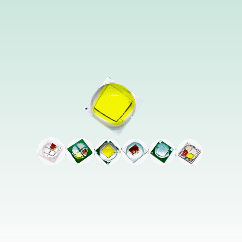
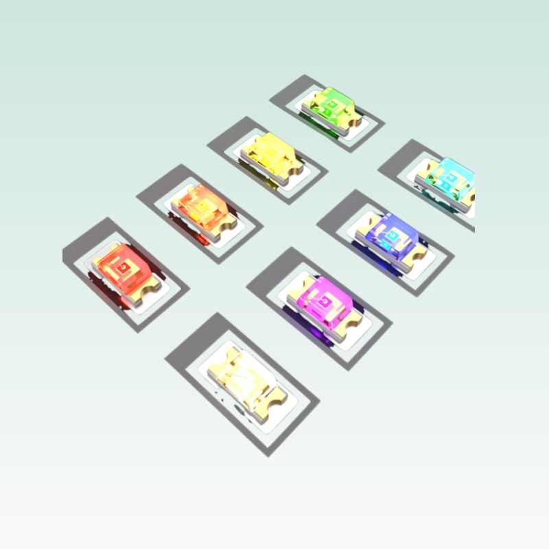
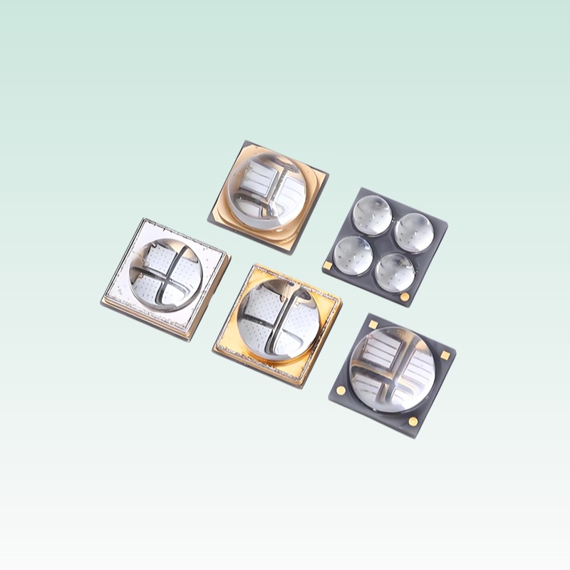
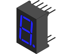
At present, the packaging types of LED products mainly include Through Hole LEDs, Surface Mounting (SMD), Direct Bonding (Direct Bonding), etc. Among them, SMD LEDs are smaller than other traditional LEDs, so SMD LEDs are mainly used for mobile phone screen backlight and mobile phone buttons, and are greatly affected by mobile phone demand.
Visible light LEDs include red, orange, yellow, green, blue, and purple LEDs. Among them, GaP (binary system), AlGaAs (ternary system) and AlGaInP (quaternary system) are the main materials for red LEDs; GaN is the main material for blue/white LEDs.
The application of LED is very extensive, mainly including:
- LED display screen: indoor and outdoor billboards, sports scoreboards, information display screens, etc.;
- Signal indicator lights: urban traffic lights, expressway, railway and airport signal lights in major and medium-sized cities across the country, and electronic equipment function indications;
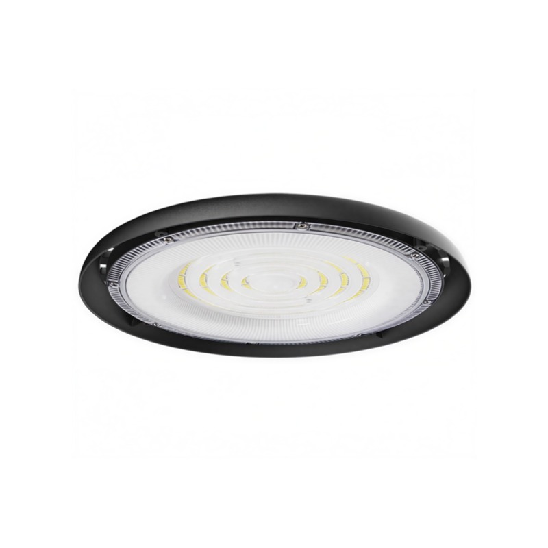
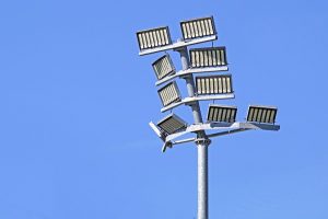
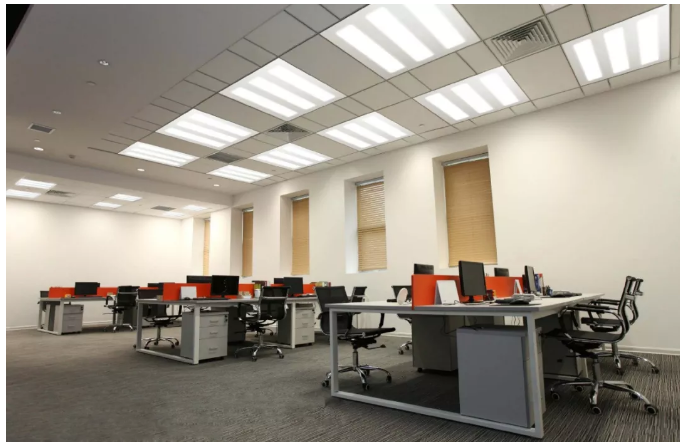
- Light color lighting: outdoor landscape lighting and interior decoration lighting;
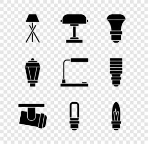
- Special general lighting: portable lighting (flashlight, headlight), low-light lighting (corridor lights, house lights, family lights), reading lighting (reading lights for airplanes, trains, and cars), microscope lights, camera flashes, desk lamps , street lights;
- Safety lighting: miner’s lamp, explosion-proof lamp, emergency lamp, safety indicator lamp;
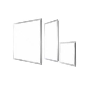
- Backlight: Backlight for LCD monitors and LCD TVs.
- Automotive lights: including interior lighting and exterior lighting. The interior of the car includes dashboards, electrical product indicators (switches, audio, etc.), switch backlights, reading lights, and external brake lights, tail lights, side lights and headlights. lights etc.
- Other applications: consumer use, such as children’s flash shoes, Christmas tree LED lights, etc.
LED industry chain
The entry threshold of the LED industry chain from upstream to downstream industries is gradually lowered. The upstream is single wafer and its epitaxy, the midstream is LED chip processing, and the downstream is packaging testing and application. Among them, the upstream and midstream areas have high technological content and high capital investment density, which are the areas with the most intense international competition and the greatest operating risks. In the LED industry chain, LED epitaxial wafers and chips account for about 70% of the industry’s profits, LED packaging accounts for about 10-20%, and LED applications account for about 10-20%.
A single wafer is the base for manufacturing LEDs, also known as a substrate, and sapphire, silicon carbide, GaAs, and GaP are mostly used as materials. Epitaxial wafers are grown on single crystals with multiple layers of single crystal films of different thicknesses, such as AlGaAs, AlGaInP, GaInN, etc., to realize LEDs of different colors or wavelengths. Common epitaxy methods include liquid phase epitaxy (LPE), vapor phase epitaxy (VPE), and metal organic chemical vapor deposition (MOCVD), among which VPE and LPE technologies are quite mature and can be used to grow LEDs with general brightness. The growth of high-brightness LED must adopt the MOCVD method. At present, the main manufacturers of MOVCD in the world are AIXTRON Company of Germany and VEECO Company of the United States. The former accounts for about 60% to 70% of the international market share, and the latter accounts for 30% to 40%. The equipment produced by Japanese manufacturers is basically limited to domestic sales in Japan.
The midstream is mainly chip design and processing. Midstream manufacturers carry out device structure and process design according to the performance requirements of LEDs, diffuse through epitaxial wafers, then metal coat, then perform photolithography, heat treatment, form metal electrodes, and then cut the substrate after grinding and polishing.
Downstream includes packaging, testing and application of LED chips. LED packaging refers to connecting the outer leads to the electrodes of the LED chip to form an LED device. The packaging plays the role of protecting the LED chip and improving the efficiency of light extraction. LED packaging technology is developed from the packaging technology of semiconductor discrete devices.
It is forbidden to use the above content without the authorization of the author, and the reprint must note the source of this content reprint or the consent of Queendom
Explore More from Queendom Lamp
Stay updated with the latest LED technology, lighting solutions, and industry insights.
Request a Quote About Queendom