





Exterior automotive lighting is the most demanding volume application for visible and near-infrared LEDs. A headlamp emitter sees −40 °C cold soaks in Scandinavia and 125 °C junction temperatures in a Saudi traffic jam, on the same part number, inside a sealed optical chamber that may also contain condensation. The qualification standard that governs these devices is AEC-Q102 (автомобильный стандарт), and understanding what it does and does not prove is the difference between a lighting design that survives its warranty period and one that returns in year three. This white paper explains the AEC-Q102 test families, shows how junction temperature drives flux maintenance, and describes how QUEENDOM’s J-01 3535 ceramic, J-02 5050 ceramic and J-03 7070 ceramic packages are being progressed against the standard. It is written for automotive lighting engineers and Tier-1 component buyers who must read a qualification report critically. Where our parts have not yet completed qualification, this paper states so explicitly: the current status of the J-01, J-02 and J-03 families is AEC-Q102 in progress.
1. Why exterior lighting needs a dedicated qualification standard
Automotive component qualification is organised by stress domain. AEC-Q100 covers integrated circuits, AEC-Q101 covers discrete semiconductors, AEC-Q200 covers passive components, and AEC-Q102 (автомобильный стандарт) — Stress Test Qualification for Discrete Optoelectronic Semiconductors in Automotive Applications — covers LEDs, photodiodes, image sensors and laser components. A visible LED is not a discrete transistor: it has an optical path, a phosphor layer, a silicone or glass encapsulant, and a package whose coefficient of thermal expansion must match a ceramic substrate across a 165 K temperature swing. Reusing AEC-Q101 test conditions would miss the failure modes that actually occur.
The two dominant field failure mechanisms in exterior LEDs are flux depreciation — a slow loss of light output driven by junction temperature and current density — and package-level fracture or delamination, driven by thermal cycling and moisture ingress. AEC-Q102 is constructed to expose both.
| Стандартная гарантия | Scope | Applies to exterior LED? |
|---|---|---|
| AEC-Q100 | Integrated circuits | No |
| AEC-Q101 | Discrete semiconductors (transistors, diodes) | No |
| AEC-Q102 (автомобильный стандарт) | Discrete optoelectronic semiconductors | Yes |
| AEC-Q200 | Passive components | No |
| IES LM-80 / TM-21 | Lumen maintenance measurement and projection | Complementary, not a substitute |
| IEC 62471 | Photobiological safety | Complementary, not a substitute |
| ISO 26262 | Functional safety (system level) | Complementary, for ADB and LiDAR |
2. How the AEC-Q102 test families stress a package
AEC-Q102 is organised into test groups that must each be run on a defined sample size with zero failures permitted for qualification. The groups are designed so that no single stress dominates: a part that survives 1,000 temperature cycles but fails damp heat has not qualified.
The test groups below are the core of the qualification programme. Sample sizes and durations are set by the standard; the table summarises what each group is designed to expose.
| Test group | Typical condition | Purpose |
|---|---|---|
| Preconditioning | Reflow simulation, 3 passes | Reproduce board assembly stress before testing |
| High-temperature operating life (HTOL) | 1,000 h at max rated current, 85–105 °C ambient | Flux depreciation, die attach fatigue |
| High-temperature storage | 1,000 h at 150 °C, unbiased | Encapsulant yellowing, wire bond intermetallics |
| Temperature cycling | −40 °C to +125 °C, 1,000 cycles | Solder joint and package fracture |
| Power temperature cycling | Current on/off with ΔTj ≈ 100 K, 1,000 cycles | Die attach delamination |
| Damp heat | 85 °C / 85 % RH, 1,000 h | Moisture ingress, phosphor degradation |
| Mechanical shock | 1,500 g, 0.5 ms, multiple axes | Wire bond and die crack |
| Vibration | Variable frequency sweep, 20–2,000 Hz | Bond fatigue |
| ESD / HBM and CDM | Per AEC-Q101 methodology | Handling and assembly robustness |
| Electro-optical parameter verification | Before, during and after each group | Confirms the part still works, not just that it survived |
2.1 Why the ceramic body changes the outcome
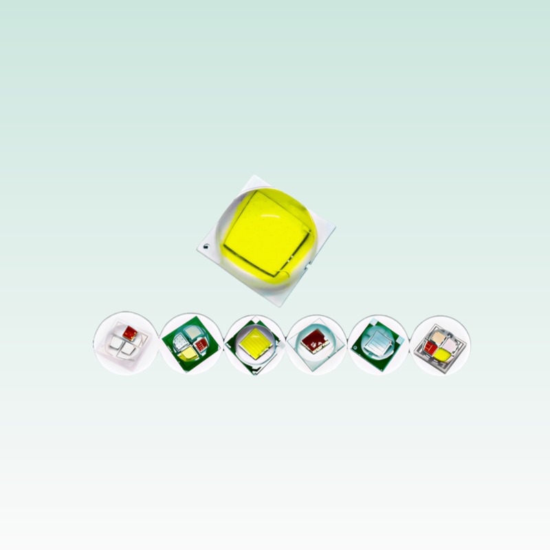
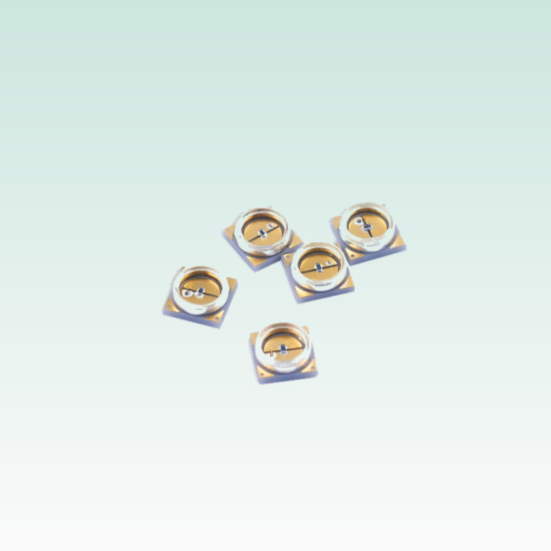
The J-01, J-02 and J-03 families use ceramic substrates — 3535, 5050 and 7070 footprints respectively — with direct-bond copper and a low thermal-resistance junction-to-case path. Three consequences follow for qualification:
- Lower junction temperature at a given drive current. A ceramic body with roughly 3–8 K/W junction-to-case resistance holds the die 20–40 K cooler than a plastic SMD part at the same current, which directly extends flux maintenance.
- Better CTE matching. Ceramic substrates sit closer to the LED die’s expansion coefficient than plastic lead-frame materials, reducing the shear stress at the die attach across a 1,000-cycle thermal cycle test.
- Higher tolerated peak current. ADB and LiDAR functions require short, high-current pulses; the ceramic body removes heat from a 1 A pulse faster than 50 mA of steady-state operation would suggest.
3. Key parameters and selection
The three parts are not interchangeable. The 3535 body suits high-resolution ADB pixel arrays and LiDAR emitters where footprint density dominates; the 5050 balances flux and area for mainstream headlamp low beam; the 7070 provides the highest flux per component for high beam and DRL functions where a smaller number of larger emitters reduces optical complexity.
| Parameter | J-01 3535 ceramic | J-02 5050 ceramic | J-03 7070 ceramic |
|---|---|---|---|
| Package footprint | 3.5 × 3.5 mm | 5.0 × 5.0 mm | 7.0 × 7.0 mm |
| Typical function | ADB pixel, LiDAR emitter | Low / high beam | High beam, DRL, position |
| Max drive current | 1.0 A pulsed | 1.5 A | 3.0 A |
| Forward voltage | 2.9–3.4 V @ 350 mA | 2.9–3.6 V @ 700 mA | 3.0–3.8 V @ 1.0 A |
| Luminous flux (white) | 120–180 lm @ 350 mA | 300–450 lm @ 700 mA | 900–1,300 lm @ 1.0 A |
| Rth junction-to-case | ~4 K/W | ~3 K/W | ~1.5 K/W |
| Viewing angle | 120° | 120° | 120° / 90° options |
| AEC-Q102 status | in progress | in progress | in progress |
| Operating ambient, rated | −40 °C to +125 °C | −40 °C to +125 °C | −40 °C to +125 °C |
3.1 Junction temperature versus flux maintenance
Flux maintenance is the fraction of initial luminous flux remaining after a given operating time. It is strongly and non-linearly dependent on junction temperature. The curves below show representative LM-80-style maintenance behaviour for the J-01, J-02 and J-03 families at their rated currents on different heat-sink temperatures. A 25 K reduction in junction temperature typically buys a factor of two to three in projected lifetime.
4. Designing for thermal cycling
Temperature cycling is where packages physically fail. A 1,000-cycle test from −40 °C to +125 °C imposes a 165 K swing on every material interface. Because ceramic, copper, solder and silicone expand at different rates, each cycle accumulates plastic strain in the weakest layer. Two design rules follow.
Keep the soldered layer thin and well wetted. A void-free solder joint of 80–120 µm transfers the shear stress more evenly than a thick or partially wetted joint. Reflow profile control is a qualification activity, not a production detail.
Respect the package CTE at the board level. A ceramic LED soldered to an FR-4 board with a high CTE mismatch will crack at the peripheral solder fillets after several hundred cycles. Metal-core PCB or a ceramic carrier with a compliant interface is the standard mitigation.
4.1 Cumulative strain versus temperature cycles
The curve below illustrates representative cumulative damage against cycle count for three solder regimes. The knee, where the curve steepens sharply, marks the onset of visible cracking and typically occurs between 200 and 500 cycles for marginal joints and beyond 1,000 cycles for well-controlled ones.
5. Product mapping for exterior functions
The table maps common exterior automotive functions onto the three ceramic families, with the optical and thermal requirement that drives the choice.
| Function | Recommended part | Why | Key requirement |
|---|---|---|---|
| Adaptive driving beam (ADB) pixel | J-01 3535 ceramic | Smallest footprint for dense emitter arrays | 1.0 A pulses, ≤ 5 K/W Rth |
| LiDAR emitter (NIR) | J-01 3535 ceramic | Fast rise time, narrow spectrum | ns-class pulse capability |
| Low beam / high beam | J-02 5050 ceramic | Flux versus area balance | 1.5 A, 300–450 lm |
| High beam, long throw | J-03 7070 ceramic | Highest flux per emitter | 3.0 A, 900–1,300 lm |
| Daytime running light (DRL) | J-03 7070 ceramic | Fewer optics, uniform bar | Continuous, thermal derating |
| Position / tail lamp | J-02 5050 ceramic | Cost-effective at moderate flux | Continuous, wide view angle |
| Front turn indicator | J-02 5050 ceramic | Amber bin control | Chromaticity stability over life |
6. Common mistakes and how to avoid them
| Mistake | Consequence | Correction |
|---|---|---|
| Treating “AEC-Q102 in progress” as qualified | Design frozen on an unqualified part | Confirm qualification status with the supplier before design freeze |
| Reading AEC-Q102 as a flux-maintenance guarantee | Lumen maintenance figure unsupported | Pair AEC-Q102 with LM-80 and TM-21 projections |
| Sizing the heat sink on steady-state current only | Junction over-temperature in pulsed ADB | Use transient thermal impedance for pulse duty |
| Ignoring reflow preconditioning | Package delamination appearing as field failure | Run the full three-pass preconditioning before any other test |
| Quoting a lifetime in years instead of hours at Tj | Comparison impossible between suppliers | Always state hours and junction temperature together |
| Using a plastic SMD part in a headlamp chamber | Accelerated yellowing and flux loss | Specify ceramic or an automotive-grade optical polymer |
| Omitting chromaticity drift from the specification | Colour shift visible over lifetime | Specify Δu′v′ limits at end of life, not only at t = 0 |
7. Verification and test methods
- Electro-optical parameter verification — measure forward voltage, luminous flux, chromaticity and view angle before, during and after each stress group, at a controlled case temperature, so that shifts are attributable to the stress rather than to the measurement fixture.
- Transient thermal characterisation — measure the junction-to-case thermal resistance and the transient impedance curve using the standard forward-voltage method. This provides the input for any pulse-mode thermal design.
- Flux maintenance — run LM-80-style testing at multiple case temperatures for at least 6,000 hours and project long-term behaviour with IES TM-21. Report the projection basis, sample size and the monitored case temperatures.
- Destructive physical analysis — after temperature cycling and damp heat, cross-section representative samples to look for die attach delamination, wire bond damage and encapsulant cracking. Survival without optical damage is not the same as survival without mechanical damage.
- System-level photometry — validate the complete lamp against the applicable regulatory photometric specification, since package-level performance does not translate directly to a sealed optical assembly.
8. Conclusion and selection guidance
For exterior automotive designs, start with the package size that matches the emitter density the optics require: J-01 3535 ceramic for ADB pixel arrays and LiDAR emitters where individual component footprint dominates, J-02 5050 ceramic for mainstream low and high beam where flux and area must be balanced, and J-03 7070 ceramic for high-flux functions such as long-throw high beam and DRL where fewer, larger emitters simplify optical design. In every case, verify the qualification status directly with the supplier before freezing a design: the current status of these families is AEC-Q102 in progress, and a design that depends on a completed qualification report should not proceed until that report exists. Pair any lifetime claim with LM-80 data and a stated junction temperature.
9. Referenced standards
- AEC-Q102 — Stress test qualification for discrete optoelectronic semiconductors in automotive applications
- AEC-Q101 — Stress test qualification for discrete semiconductors
- IES LM-80 — Approved method: measuring luminous flux maintenance of LED light sources
- IES TM-21 — Projecting long-term lumen maintenance of LED light sources
- IEC 62471 — Photobiological safety of lamps and lamp systems
- ISO 26262 — Road vehicles: functional safety
- SAE J1383 — Performance requirements for replacement light sources in automotive applications
- CIE 127 — Measurement of LEDs
10. Contact us
QUEENDOM supplies the J-01 3535 ceramic, J-02 5050 ceramic and J-03 7070 ceramic families from stock, with reference thermal designs, transient thermal impedance data and binning information for automotive optical design. Our component engineering group can discuss the AEC-Q102 qualification programme for these parts on request and will state the current status of the programme plainly. Note that these families are currently AEC-Q102 in progress; parts should be specified accordingly. Contact us for samples, thermal models and application support.
Related products and applications
The ceramic automotive packages discussed here are available in the following product families.
- High-power SMD LED (J-01)
- High-power SMD LED (J-02)
- High-power SMD LED (J-03)
- Application overview: LED components application solutions
- More technical papers: LED knowledge resources