








Two LEDs from the same reel can fail in ways that look similar to a customer and are completely different to an engineer. One was destroyed by a 2 kV discharge from a charged operator to the die, in a few nanoseconds, after which it behaved as a resistor. The other was destroyed by an over-current condition that persisted for milliseconds and cooked the wire bond. Both arrive as “the LED failed on the board”. This page sets out the damage criteria that separate electrostatic discharge from electrical over-stress, the classification system used to specify ESD robustness, and the production protections that keep both failure modes out of a finished luminaire. It is written for production engineers, quality staff and buyers who must write handling and process specifications for ceramic high-power, infrared and UV-C parts.
1. Why the distinction matters commercially
ESD and EOS are often treated as one subject, grouped under a single “handle with care” instruction. That grouping hides the fact that they have different causes, different controls and different cost structures. ESD is a transient energy event arising from charged objects and people; it is controlled by grounding, materials and packaging, and it costs relatively little to prevent. EOS is a sustained energy event arising from the drive circuit, a mis-mated connector, a test fixture error or a soldering fault; it is controlled by circuit design, current limiting and process discipline.
Getting the diagnosis wrong leads to the wrong corrective action being paid for. A line that installs a full electrostatic protected area in response to an EOS problem has spent capital and changed nothing. A line that blames the customer’s driver for an ESD problem has left an ungrounded handling station in production. Since the two damage morphologies are distinguishable under inspection and by electrical signature, the correct first step is always characterisation, not assumption.
| Observation at return | Points toward ESD | Points toward EOS |
|---|---|---|
| Failure distribution across a reel | Scattered, low fraction | Clustered at a process step or fixture |
| Timing of failure | At assembly, before first power | After first power or during burn-in |
| Die appearance | Localised melt pit at bond pad | Diffuse melting, sometimes wire fused |
| Wire bond | Usually intact | Frequently fused, ball-lifted or vaporised |
| Encapsulant | Rarely discoloured | Often discoloured above the die |
| Forward voltage | Near-open, or high and unstable | Short circuit, or low-resistance path |
| Correlation with operator / shift | Possible | Unlikely |
| Correlation with driver design | Unlikely | Common |
| Cost element | ESD control | EOS control |
|---|---|---|
| Principal capital | Wrist straps, mats, ionisers, flooring, testers | Current-limited drivers, fixture design |
| Principal operating cost | Auditing, training, compliance testing | Process control, incoming driver test |
| Typical root cause | Ungrounded station, wrong packaging | Wrong resistor, mis-sequenced power-up |
| Detection method | ESD event detector, station audit | Oscilloscope capture of current |
| Failure visibility | Often invisible until after assembly | Usually immediate and repeatable |
2. Damage physics: what the electrical event does to the die
An LED is a diode with a small active area, a thin epitaxial stack, and a metallisation and bond-pad structure whose current-carrying capacity is set by geometry. Both ESD and EOS deliver energy that the die converts into heat and into current density above the design limit, but the time constants differ by roughly six orders of magnitude, and the resulting damage geometry follows the time constant.
An electrostatic discharge transfers a small amount of stored charge in a very short time. A human body model event is a few nanocoulombs delivered in a few nanoseconds; the instantaneous power can be tens of kilowatts but the total energy is millijoules. Because the energy is delivered faster than heat can diffuse, the damage is localised: a microscopic melt channel forms at the point where current density is highest, typically at the edge of the bond pad or across the passivation to the semiconductor, and the die acquires a resistive leakage path. The melt pit is invisible without a microscope, and the wire bond is usually undamaged because it is not in the highest current-density path.
An electrical over-stress delivers far more total energy over milliseconds or longer. Heat has time to diffuse, so the damage is diffuse and thermal: the die-attach solder or epoxy can degrade, the wire bond can fuse, the encapsulant above the die can discolour, and the metallisation can be consumed over a wide area. The bond wire is frequently the limiting element and fails open.
The physical origin of each event also differs. ESD events are generated by triboelectric charging — a person walking on a synthetic floor, a board sliding out of a plastic bag, a tape-and-reel cover peeling off — followed by a discharge to a device. EOS originates in circuit conditions: a driver with insufficient series resistance, an inductor in the output, a supply sequenced before the control ground, a test probe touching the wrong pad, or a soldering iron tip carrying mains leakage.
Both damage types are also cumulative in the sense that partial ESD damage produces a latent defect: the device passes final test but has a reduced lifetime because the leakage path is thermally unstable. Latent ESD damage is the reason that final electrical test is not a sufficient ESD control.
3. Reverse behaviour: the second diagnostic axis
Forward I-V alone does not separate the two mechanisms reliably, because a badly damaged ESD part can look like an EOS part. The reverse characteristic adds the discriminating information. A healthy LED blocks reverse voltage until its rating, with leakage in the nanoampere range. An ESD-damaged die typically shows elevated reverse leakage — microamperes to milliamperes at a fraction of rated reverse voltage — with a soft, non-destructive breakdown and a strong temperature dependence. A severe EOS event usually produces a hard short, and the reverse curve is a low-resistance line through the origin.
Plotting both directions and comparing the two curves is therefore the standard first-line electrical screen, and it is non-destructive: it can be performed on every unit at final test and on returned parts before any de-processing.
| Test | Condition | Healthy result | ESD damage signature | EOS damage signature |
|---|---|---|---|---|
| Forward Vf | Rated current, 25 °C | Within bin, ± 0.1 V | + 0.05 to + 0.4 V, soft knee | – 0.3 V and below, or open |
| Forward leakage | 0.1 × rated Vf | < 1 µA | 1 µA to 1 mA | Short, mA to A |
| Reverse leakage | 5 V reverse | < 0.1 µA | 0.1 µA to 1 mA, unstable | Short circuit |
| Reverse breakdown | Ramp to rating | Flat at rating | Lower, soft | Not measurable |
| Curve shape | Swept I-V | Sharp exponential knee | Two-slope, series resistance | Near-linear, resistive |
| Temperature coefficient | Vf vs 25 / 85 °C | – 2 to – 4 mV/K | Anomalous, low | Near zero |
| Optical output | At rated current | Within bin | Reduced, sometimes 10–40 % | Zero or near zero |
4. Classification: HBM, MM and CDM
The industry classifies a component’s ESD robustness by exposing samples to a defined discharge waveform and recording the highest voltage at which the part survives. Three models are used, and a specification that states a single number without naming the model is incomplete.
| Modello | Abbreviation | Simulates | Waveform | Garanzia Standard | Typical LED withstand |
|---|---|---|---|---|---|
| Human body model | HBM | Charged person touching a device | 100 pF, 1.5 kΩ, rise 2–10 ns, decay ~150 ns | ANSI/ESDA/JEDEC JS-001 | 1–8 kV |
| Machine model | MM | Charged metal tool or fixture | 200 pF, ~0 Ω, oscillatory, ~15 ns | JESD22-A115 | 100–800 V |
| Charged device model | CDM | Device itself charged then discharged | Device capacitance, < 1 Ω, rise < 1 ns | ANSI/ESDA/JEDEC JS-002 | 250–2000 V |
The three are not interchangeable and cannot be converted by a fixed ratio, although the familiar industry approximation of MM ≈ HBM / 10 is sometimes used for rough comparison. CDM is the model most relevant to automated assembly, because a device sliding down a feeder or a nozzle picks up charge and then discharges the instant it touches a grounded surface; the extremely fast rise time means CDM events are the hardest to protect against and the ones most likely to cause the localised melt pit described earlier.
| Device class | HBM withstand | MM withstand | CDM withstand | Handling requirement |
|---|---|---|---|---|
| Class 0 | < 250 V | < 100 V | < 125 V | Full EPA, ionised air, no manual contact |
| Class 1A | 250–499 V | 100–199 V | 125–249 V | Full EPA, wrist strap, ionisers |
| Class 1B | 500–999 V | 200–399 V | 250–499 V | Full EPA, wrist strap |
| Class 1C | 1,000–1,999 V | 400–799 V | 500–999 V | EPA, wrist strap, protected packaging |
| Class 2 | 2,000–3,999 V | 800–1,999 V | ≥ 1,000 V | EPA with standard controls |
| Class 3A | 4,000–7,999 V | ≥ 2,000 V | ≥ 1,000 V | Basic ESD awareness |
| Class 3B | ≥ 8,000 V | ≥ 2,000 V | ≥ 1,000 V | Basic ESD awareness |
Ceramic high-power and UV parts generally sit in the lower classes, because the die area is small and the epitaxial structure is optimised for optical output rather than for ruggedness. High-power ceramic packages are typically Class 1B to Class 2 for HBM, while UV-C parts are often Class 1A, which is why UV-C assembly areas should be treated as high-risk electrostatic environments irrespective of the general plant classification.
5. Production protection: a layered programme
An effective programme has four layers: eliminate charge generation, drain charge that is generated, neutralise charge that cannot be drained, and verify that the first three still work. No single measure is sufficient.
| Layer | Measure | Target or limit | Verification frequency |
|---|---|---|---|
| 1 Eliminate | Replace insulators near devices (no bare plastics) | No insulator within 30 cm of device | Layout review, annual audit |
| 1 Eliminate | Humidity control in assembly area | ≥ 40 % RH | Continuous monitoring |
| 2 Drain | Wrist strap system, continuous monitor | 1 MΩ series, continuity alarm | Daily wearer test, live monitor |
| 2 Drain | Dissipative work surface | 1 × 10⁶ to 1 × 10⁹ Ω | Monthly resistance test |
| 2 Drain | Conductive flooring and footwear | < 1 × 10⁹ Ω (footwear system) | Monthly, plus daily self-test |
| 2 Drain | Equipment and tool grounding | < 1 Ω to EPA earth | Monthly bond test |
| 3 Neutralise | Ionisers at forced-air and manual stations | ± 35 V balance, decay < 5 s | Monthly balance and decay test |
| 3 Neutralise | Ionised air in feeder and tape peel zones | Decay < 10 s at 15 cm | Quarterly |
| 4 Verify | ESD event detectors on sensitive tools | Zero events per shift | Continuous |
| 4 Verify | Packaging compliance test | Surface resistance 1 × 10⁴ to 1 × 10¹¹ Ω | Per lot |
The grounding resistance limits are not arbitrary. The 1 MΩ series resistor in a wrist strap is a safety requirement: it limits the current that could pass through a wearer in the event of accidental contact with mains voltage, while still draining charge fast enough to protect a Class 0 device. A wrist strap tested with a simple continuity beeper is not verified; the test must measure resistance and confirm it lies inside the specified window, because both an open strap and a shorted strap are hazardous, one to the device and one to the operator.
| Grounding parameter | Limit | Rationale | Test method |
|---|---|---|---|
| Wrist strap system resistance | 7.5 × 10⁵ to 3.5 × 10⁷ Ω | Safety current limit plus charge decay | Wearer test, calibrated meter |
| Wrist strap cord resistance | 1 × 10⁶ Ω nominal | Operator safety | Component test |
| Common point ground to earth | < 1 Ω | Low-impedance reference | Bond tester, 1 A |
| Work surface to ground | 1 × 10⁶ to 1 × 10⁹ Ω | Charge decay without shock risk | Surface resistance meter |
| Floor to ground | < 1 × 10⁹ Ω | Footwear system | Floor resistance meter |
| Dissipative container | 1 × 10⁴ to 1 × 10¹¹ Ω | Drain while cushioning | Per ASTM D257 method |
| Ioniser offset voltage | ± 35 V | Prevent induced charge | Charged plate monitor |
| Ioniser decay time | < 5 s from ± 1,000 V to ± 100 V | Throughput compatibility | Charged plate monitor |
6. Part-family guidance
The three families in scope have different exposure profiles, so the protection programme should not be identical for all of them.
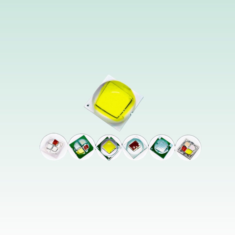
J-01 (3535 ceramic) is a visible high-power ceramic part used in automotive and machine-vision applications. The ceramic body is robust mechanically and immune to the moisture-related ESD problems of plastic packages, but the small die and the eutectic die attach mean a CDM event can damage the die-attach interface as well as the junction. Given the automotive track, incoming and in-process handling should be within a full electrostatic protected area, and the supplier’s HBM and CDM classification should be on the datasheet and confirmed by the part’s qualification data.
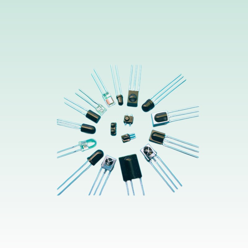
J-05 (2835 infrared) is a volume plastic-bodied infrared part, frequently placed on boards that also carry exposed pads and connectors. The package’s plastic body can itself hold charge, which makes CDM events during tape-and-reel feeding a realistic risk. Because these parts are often used in high volume, they are also most likely to be placed on equipment that was never evaluated for ESD, such as older pick-and-place feeders without ionisation.
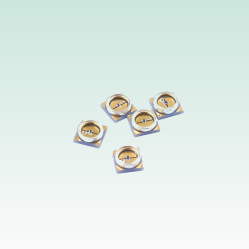
J-15 (3535 UVC, 275 nm) is the most ESD-sensitive part in the group. The wide-bandgap semiconductor structure of a deep-ultraviolet LED has a lower tolerance for the current filaments that an ESD event produces, and the part’s low HBM class reflects that. UVC assembly should be treated as a high-risk electrostatic area even if the plant classification is lower, with ionised air at every manual station, no manual lead forming, and no direct contact with the package aperture.
Separation note. The 254 nm technology in this product portfolio is the Z-14 mercury lamp tube, not an LED. It is a glass envelope device with a different failure and handling profile, and it must not be grouped with the J-15 LED in an ESD control plan or in a test specification.
| Part | Package | Class (typical) | Key risk during assembly | Priority control |
|---|---|---|---|---|
| J-01 3535 Ceramic | AlN ceramic, visible | HBM Class 1B–2 | CDM at die attach, no plastic to absorb charge | Full EPA, ionisers, verified wrist straps |
| J-05 2835 Infrared | 2835 plastic SMD | HBM Class 1B–2 | Plastic body charge, feeder discharge | Ionised feeders, dissipative reels |
| J-15 3535 UVC | AlN ceramic, 275 nm | HBM Class 1A | Lowest ESD tolerance, aperture contamination | Full EPA, no manual contact, live monitors |
7. Process control points that prevent EOS
EOS is not prevented by an electrostatic programme, so it needs its own controls. The following points account for most production EOS incidents in LED assemblies.
The first is driver current limiting. Every test source used to power an LED during assembly must be a current-limited source set to the rated current or below, never a voltage source relying on the LED’s own impedance. A voltage source into a 3 V die with no series resistance will deliver whatever the source can supply, which is EOS by design.
The second is power sequencing. Where a board has both a control supply and an LED supply, the control supply must be established first and removed last, so that the driver output stage never presents an indeterminate state to the LED string.
The third is test fixture integrity. Spring probes that bounce, connectors that are mated under load, and fixtures with long unshielded leads carrying switching transients are all common EOS sources. Capturing the current waveform at the LED with a current probe during first power-on is the only reliable way to prove that the fixture does not over-stress the part.
The fourth is soldering and rework discipline. A soldering iron with mains leakage current, an ungrounded iron, or a rework station with a floating tip applies an uncontrolled voltage to the die through the lead frame. Both the EOS and the ESD programme depend on iron tips that are grounded through a resistance and verified.
| EOS source | Mechanism | Control | Verification |
|---|---|---|---|
| Voltage-mode test source | Unlimited current into 3 V die | Current-limited supply at rated current | Setting sheet, fixture photo |
| Power-up sequencing | Driver output indeterminate | Control rail first, LED rail last | Sequence test on first article |
| Inductive drive transients | Back-EMF above reverse rating | Clamp diode, damped output | Oscilloscope capture |
| Bouncing test probes | Intermittent make-break arcs | Probe planarity, spring force specification | Fixture maintenance log |
| ESD-damaged die under load | Latent leakage initiates thermal runaway | ESD control upstream | Return analysis |
| Ungrounded soldering iron | Mains leakage through tip | Grounded, verified iron tip | Daily tip-to-ground test |
| Static into connector during mating | Charge transfer to LED string | Ionised station, mate unpowered | Station audit |
8. Diagnosis workflow for a returned part
Working through a returned LED systematically is faster than guessing, and it produces evidence a customer will accept.
- Record the context. Ask for the assembly date, the process step at which the failure appeared, the drive conditions, and whether the failure was immediate or after some operating time. This alone separates many ESD from EOS cases before any measurement.
- Screen electrically at fixed temperature. Measure forward Vf at rated current and reverse leakage at a fraction of reverse rating, at a controlled temperature. Compare against a known-good reference from the same bin, not against a datasheet typical.
- Characterise optically. Measure flux and peak wavelength at the same current and case temperature as the reference. A part that is electrically near-normal but optically low usually has an encapsulant or extraction problem rather than an electrical one.
- Inspect non-destructively. Optical microscopy at 50–200× looks for the melt pit, discolouration and bond geometry. X-ray reveals bond lift or fusing and die-attach voiding.
- De-process and analyse. Decapsulate, then examine with SEM and EDS. A localised melt pit at the pad edge with intact wire is the ESD signature; diffuse melting, a fused or vaporised wire, and carbonised encapsulant are the EOS signature.
- Reproduce. Where the customer’s process can be instrumented, capture the current and voltage waveform at the LED during the identified process step and compare the energy delivered against the part’s rating. A diagnosis that cannot be reproduced cannot be corrected.
9. Selection and specification guidance
When specifying an LED for a new design, the ESD and EOS requirements should be written into the purchase specification rather than left to assumption. The specification should state the required HBM, MM and CDM classification with the test standard named, and should require the classification on the datasheet rather than in a private report. It should state the maximum reverse voltage that the application will present, including transients, and require a margin of at least two to one against that figure. It should define the packaging requirement — dissipative tape and reel, moisture barrier bag with an ESD warning — because the packaging is part of the protection programme.
For the parts in this family, the practical guidance is to treat J-15 (3535 UVC, 275 nm) at the highest control level, J-01 (3535 ceramic) at a full electrostatic protected area level with CDM attention at the die attach, and J-05 (2835 infrared) with particular attention to feeder and reel charge generation. None of the three should be handled outside an electrostatic protected area, and no part in this family should be powered from a voltage source without a verified current limit. Where the automotive route applies to the ceramic parts, note that the automotive qualification status is AEC-Q102 in progress and that ESD classification data supports the reliability case but is not itself a qualification certificate.
10. Referenced standards
- ANSI/ESDA/JEDEC JS-001 — For electrostatic discharge sensitivity testing, human body model component level
- ANSI/ESDA/JEDEC JS-002 — For electrostatic discharge sensitivity testing, charged device model component level
- JESD22-A114 — Electrostatic discharge sensitivity testing, human body model
- JESD22-A115 — Electrostatic discharge sensitivity testing, machine model
- IEC 61340-5-1 — Protection of electronic devices from electrostatic phenomena: general requirements
- IEC 61340-5-2 — Protection of electronic devices from electrostatic phenomena: user guide
- IEC 61000-4-2 — Testing and measurement techniques: electrostatic discharge immunity test
- JESD22-A101 — Steady state temperature humidity bias life test
- AEC-Q102 — Stress test qualification for automotive discrete optoelectronic semiconductors
11. Contact us and sample requests
QUEENDOM’s component engineering group supports ESD and EOS investigations for the ceramic, infrared and UV-C lines with electrical characterisation, optical measurement, X-ray imaging and, where required, decapsulation for SEM and EDS analysis. When requesting support or samples, provide the assembly process flow, the drive circuit schematic or at least its topology, the point in the process at which the failure appears, and the datasheet classification of the failed part, so that the comparison against a known-good reference is meaningful and the corrective action can be targeted at the correct mechanism.
Related products and applications
The packages and the production-protection parts referenced here are listed below.
- High-power SMD LED (J-01)
- Infrared emitter LED (J-05)
- UVC 275 nm LED (J-15)
- Application overview: LED components application solutions
- More technical papers: LED knowledge resources