

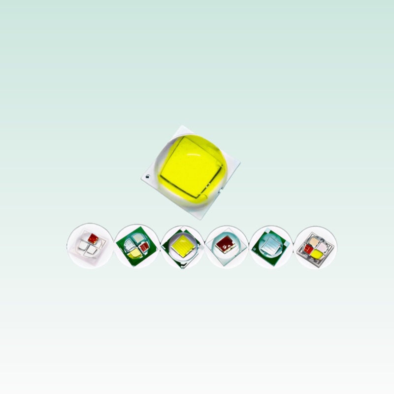
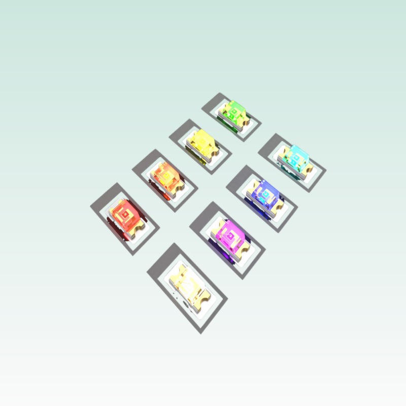
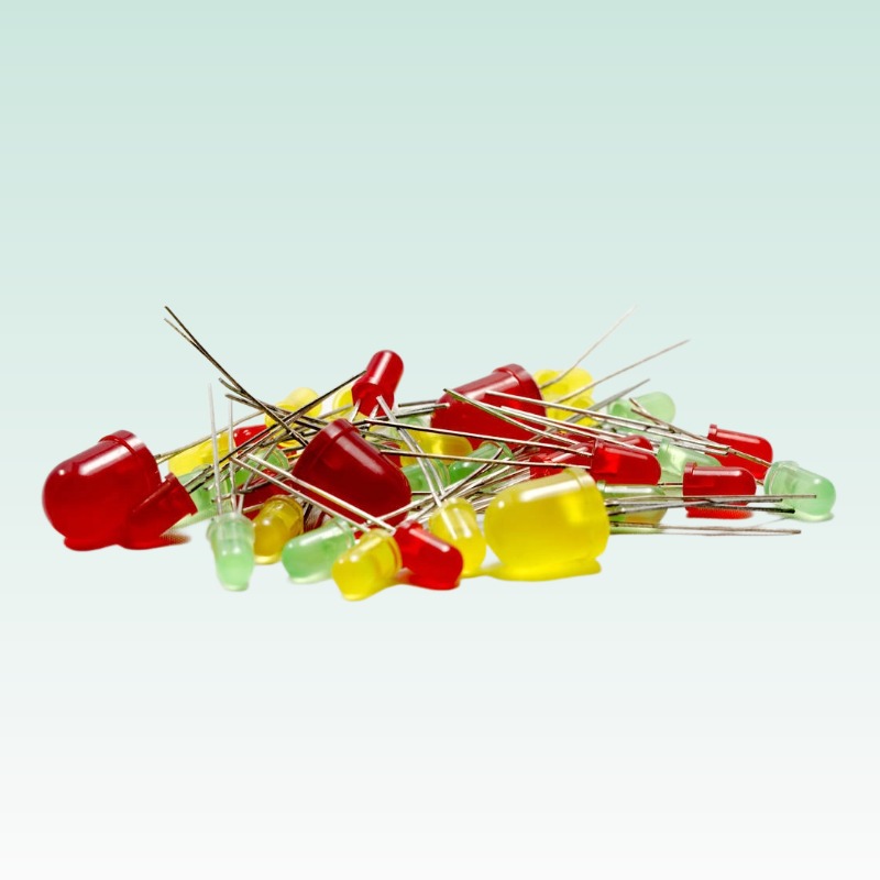
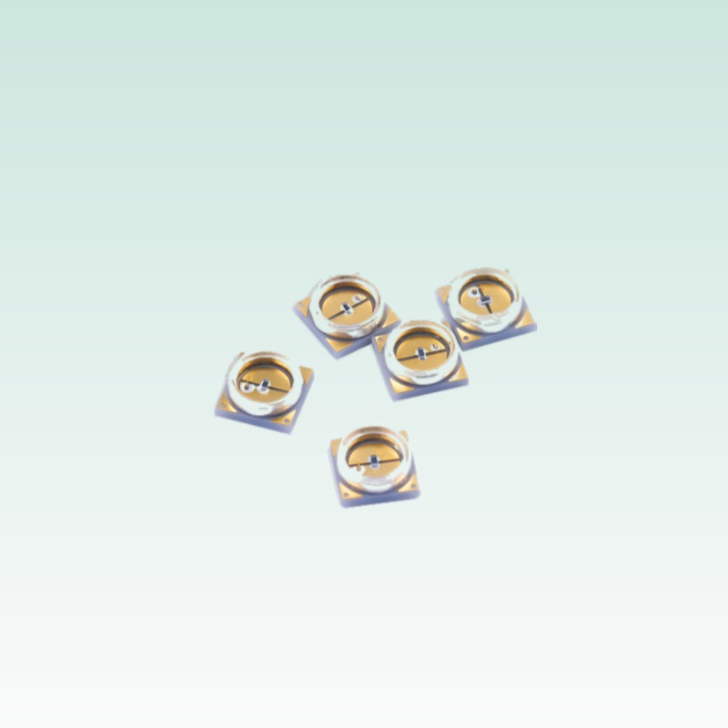





Ultraviolet-A is the workhorse band of industrial photochemistry. Adhesives, coatings, inks and 3D-printing resins are cured by it; fluorescence inspection, document security, leak detection and machine-vision marking are all built on it. The engineering question is almost never “do we need UVA” but “which UVA wavelength”, and the answer is set by the absorption spectrum of the photoinitiator or fluorophore, not by the emitter’s price. This white paper is written for process engineers and machine designers specifying UVA sources, and it works through the four wavelengths that dominate the market — 365, 375, 385 and 405 nm — using QUEENDOM’s J-12 3535 UVA (365/375/385 nm), J-11 2835 UVA (405 nm) and J-10 3 mm UVA (405 nm) families as the reference parts.
1. Why the wavelength choice is a chemistry decision
A UV-curable formulation contains a photoinitiator, sometimes several, plus oligomers and monomers. The photoinitiator absorbs photons in a specific band and, once excited, fragments into radicals that begin polymerisation. If the emitter’s output does not overlap the photoinitiator’s absorption band, no matter how much power is delivered, nothing cures.
This single fact explains most field failures in UV LED conversions. A process that ran for years under a broadband mercury lamp may be built around a photoinitiator that absorbs broadly across 250–400 nm. Replacing the lamp with a 405 nm LED array removes all the short-wavelength energy the chemistry was using, and the coating emerges tacky. The retrofit is not a power problem; it is a spectral mismatch.
| الطول الموجي | Photon energy (eV) | Typical photoinitiator match | Typical application |
|---|---|---|---|
| 365 nm | 3.40 | TPO, ITX, some benzophenone systems | Deepest cure, thick films, adhesives |
| 375 nm | 3.31 | TPO, blends | General-purpose curing |
| 385 nm | 3.22 | TPO, BAPO, blends | Coatings and inks |
| 395 nm | 3.14 | BAPO, blends | Inks, 3D printing |
| 405 nm | 3.06 | BAPO, titanocene, visible-light initiators | Inks, 3D printing, sensing |
The trade-off runs in one direction: shorter wavelength means higher photon energy and better through-cure, but also lower wall-plug efficiency, higher cost per watt and greater biological hazard. The 405 nm emitter is efficient, inexpensive and safe enough to be treated more like a visible light source; the 365 nm emitter is none of those things but cures films the 405 nm device cannot reach.
2. Spectral matching to the photoinitiator
The foundational design step is to overlay the emitter spectrum on the photoinitiator absorption spectrum. The overlap integral determines the fraction of emitted photons that do useful work.
The figure shows the practical situation clearly. A well-chosen photoinitiator has a broad absorption envelope, and all three emitters overlap it, but the overlap per unit power is greatest for the 365 nm device and least for the 405 nm device. When the formulation is optimised for 365 nm — as many legacy mercury-lamp formulations are — a 405 nm retrofit loses a substantial part of its useful photon flux.
| Design action | Purpose | How to verify |
|---|---|---|
| Obtain the photoinitiator absorption spectrum | Establish the target band | Supplier datasheet or spectrophotometer measurement |
| Overlay emitter spectrum | Compute spectral overlap | Normalise both to the same axis |
| Compute overlap integral | Quantify useful photon fraction | Weighted sum across the band |
| Compare at equal electrical power | Fair emitter comparison | Multiply overlap by wall-plug efficiency |
| Confirm with a cure trial | Validate the calculation | Tack-free time and depth-of-cure measurement |
3. Emitter comparison and selection
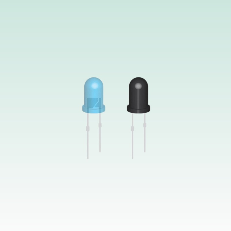
The three families serve different roles. The J-12 3535 ceramic package offers 365, 375 and 385 nm options with the flux and thermal performance needed for curing systems. The J-11 2835 UVA at 405 nm brings a compact surface-mount footprint for dense arrays, and the J-10 3 mm UVA at 405 nm suits through-hole mounting, point sensing and low-count applications.
| Parameter | J-12 3535 UVA | J-11 2835 UVA | J-10 3 mm UVA |
|---|---|---|---|
| Wavelength options | 365 / 375 / 385 nm | 405 nm | 405 nm |
| FWHM | ≤ 12–16 nm | ≤ 18 nm | ≤ 20 nm |
| Radiant flux | 350–900 mW @ 500 mA (varies by bin) | 150–350 mW @ 350 mA | 60–120 mW @ 20 mA |
| Forward voltage | 3.4–3.9 V @ 500 mA | 3.0–3.4 V @ 350 mA | 3.0–3.4 V @ 20 mA |
| Package | 3.5 × 3.5 mm ceramic, quartz window | 2835 SMD | 3 mm through-hole |
| Viewing angle | 120° | 120° | 15°–30° (lensed) |
| Thermal resistance | ~8 K/W | ~45 K/W | ~250 K/W |
| Wall-plug efficiency | 15–25 % (385 nm), 8–15 % (365 nm) | 30–40 % | 25–35 % |
| Primary use | UV curing, high-irradiance arrays | Dense curing arrays, sensing | Point sensing, fluorescence excitation |
| Ozone generation | None at these wavelengths | عدم تحديد شيء | عدم تحديد شيء |
3.1 Radiant flux versus drive current
UVA emitters show a sub-linear flux-current relationship and a pronounced thermal rollover at high current. The curve below shows representative radiant flux against drive current for the three families, with the practical operating window marked. Driving beyond the marked region buys little additional flux while sharply reducing lifetime.
4. Cure depth and dose
Cure depth follows a Beer-Lambert-style attenuation. Photon flux falls exponentially with depth as the photoinitiator and pigments absorb it, and polymerisation only occurs where the local dose exceeds the threshold needed to consume the inhibitor and gel the resin.
“ I(z) = I0 · exp(-α · z) → z = ln(I0 / I_threshold) / α “
where I(z) is irradiance at depth z, α is the effective absorption coefficient of the formulation, and z is the maximum cure depth when I(z) falls to the threshold irradiance. Practically, cure depth is not linear in irradiance: doubling irradiance does not double depth, it increases depth by a constant amount determined by ln(2) / α.
| Formulation type | Effective absorption coefficient α (mm⁻¹) | Cure depth at 1 J/cm², 365 nm | Cure depth at 1 J/cm², 405 nm |
|---|---|---|---|
| Clear acrylate adhesive | 0.6–1.0 | 3–5 mm | 2–3.5 mm |
| Clear epoxy, UV-cure | 1.0–1.8 | 1.5–3 mm | 1–2 mm |
| Lightly pigmented coating | 3–6 | 0.4–0.9 mm | 0.25–0.6 mm |
| White pigmented coating | 8–15 | 0.15–0.35 mm | 0.08–0.2 mm |
| Black pigmented ink | 20–40 | 0.05–0.15 mm | 0.03–0.09 mm |
| Filled potting compound | 5–12 | 0.2–0.5 mm | 0.12–0.35 mm |
The pattern is consistent: for every formulation class, the 365 nm source cures deeper than the 405 nm source at the same delivered dose, because the shorter wavelength is absorbed less strongly by the matrix and has higher photon energy. Pigments in particular absorb short wavelengths strongly, which is why white and black coatings cure only in thin layers regardless of the source.
| Pigment / substrate | Transmission at 365 nm | Transmission at 385 nm | Transmission at 405 nm |
|---|---|---|---|
| Unfilled clear resin, 2 mm | 88 % | 91 % | 93 % |
| Light amber resin, 2 mm | 62 % | 74 % | 84 % |
| White TiO₂-filled, 0.5 mm | 18 % | 26 % | 34 % |
| Black carbon-filled, 0.2 mm | 6 % | 9 % | 12 % |
| Polycarbonate cover, 3 mm | 0 % | 62 % | 84 % |
| Soda-lime glass, 3 mm | 78 % | 84 % | 88 % |
| Quartz window, 3 mm | 92 % | 92 % | 92 % |
Polycarbonate deserves special attention. It is effectively opaque below about 380 nm and reasonably transparent at 405 nm, which is why devices that must shine through a polycarbonate window use 405 nm emitters regardless of the cure-depth penalty.
4.1 Cure depth versus delivered dose
The curve below shows depth of cure against delivered dose for three formulations, at 365 nm and at 405 nm. The logarithmic shape means that the first 200 mJ/cm² buys most of the available depth, and further dose adds only marginally.
5. Sensing applications
UVA sensing uses the same emitters in a different role: as excitation sources rather than curing sources. The requirements differ in three ways. First, output stability matters more than output magnitude, because the measurement is a ratio. Second, ambient rejection matters, which usually means modulating the emitter and using synchronous detection. Third, the emitter is often paired with a filter and photodiode in a fixed geometry.
| Sensing application | Recommended part | الطول الموجي | Why this choice |
|---|---|---|---|
| Fluorescence inspection | J-12 3535 UVA | 365 nm | Excites most fluorophores efficiently |
| Document and currency security | J-12 3535 UVA | 365 nm | Standard excitation for security inks |
| Leak detection (fluorescent dye) | J-12 3535 UVA | 365 nm | Matches dye absorption peak |
| Machine-vision marking | J-11 2835 UVA | 405 nm | Efficient, compact array, visible alignment |
| UV curable resin depth sensing | J-11 2835 UVA | 405 nm | Low hazard, high stability |
| Through-polycarbonate cover sensing | J-11 2835 UVA | 405 nm | Only band that transmits the cover |
| Point fluorescence probe | J-10 3 mm UVA | 405 nm | Lensed narrow beam, low count |
| Optical encoder / edge detection | J-10 3 mm UVA | 405 nm | Compact through-hole source |
5.1 Eye safety and handling
All four wavelengths are within the UVA band and are classified under IEC 62471. None of them is germicidal and none generates ozone in normal operation, which distinguishes them clearly from UVB and UVC sources. Nonetheless, 365 nm carries a substantially higher actinic risk than 405 nm, and direct viewing of either is hazardous.
| Property | 365 nm | 375 nm | 385 nm | 405 nm |
|---|---|---|---|---|
| Visible to the human eye | Barely — dim violet | Faint violet | Dim violet | Clearly visible violet |
| Typical IEC 62471 risk group (single emitter) | RG2 at high flux | RG2 | RG1–RG2 | RG1 |
| Ozone generation | عدم تحديد شيء | عدم تحديد شيء | عدم تحديد شيء | عدم تحديد شيء |
| Germicidal efficacy | عدم تحديد شيء | عدم تحديد شيء | عدم تحديد شيء | عدم تحديد شيء |
| Eye protection | Required — UV goggles | مطلوب | Recommended | Recommended for extended viewing |
| Skin exposure | Avoid prolonged direct exposure | Avoid | Low risk | Low risk |
A note on a common confusion: because 405 nm is visible, users frequently assume it is safe and treat it like a blue-violet indicator light. High-flux 405 nm arrays intended for curing are not indicator lights, and the hazard scales with irradiance rather than with visibility.
6. Common mistakes and how to avoid them
| Mistake | Consequence | Correction |
|---|---|---|
| Retrofitting 405 nm into a 365 nm formulation | Coating stays tacky, cure fails | Check the photoinitiator absorption band before specifying |
| Comparing emitters on electrical power alone | Wrong emitter chosen | Compare on the overlap integral times wall-plug efficiency |
| Expecting cure depth to scale linearly with dose | Over-specified, over-heated system | Design on the logarithmic depth-dose curve |
| Ignoring pigment loading | Only a thin skin cures | Match the source to the film thickness and pigment |
| Shining through polycarbonate with a 365 nm source | Essentially no transmission | Use 405 nm when a polycarbonate window is present |
| No filter on the sensing photodiode | Ambient violet light corrupts the reading | Add a bandpass filter matched to the emitter |
| Running the 3535 part beyond rated current | Thermal rollover, reduced lifetime | Respect the recommended maximum continuous current |
| Treating high-flux 405 nm as a safe indicator source | Potential eye hazard in the work area | Classify the installed array under IEC 62471 |
7. Verification and test methods
- Spectral irradiance measurement — measure peak wavelength, FWHM and irradiance at the working plane with a calibrated spectroradiometer. UVA calibrations must be traceable; broadband radiometers with poor UV response are a common source of error.
- Dose measurement in the process — measure delivered dose in mJ/cm² at the cure plane with a radiometer designed for the specific wavelength band, and record it per production run.
- Cure depth and degree of cure — verify with a depth-of-cure test such as FTIR conversion measurement or a solvent-swipe tack test on cross-sections, rather than a surface touch test alone.
- Emitter aging — run an LM-80-style maintenance test at rated current and case temperature, and project with IES TM-21. UVA emitters in curing systems are often driven hard, so the projection basis must match the actual duty cycle.
- Uniformity mapping — map irradiance across the cure plane on a grid and report the maximum-to-minimum ratio, since non-uniform irradiance leaves uncured regions that appear as defects.
- Sensing stability — for sensing applications, log emitter output over at least 1,000 hours of duty and quantify drift, since the measurement accuracy depends directly on source stability.
8. Conclusion and selection guidance
Start from the chemistry. Obtain the photoinitiator or fluorophore absorption spectrum, overlay it on candidate emitter spectra, and compute the overlap. Then choose the part that maximises useful photon flux per unit of electrical power, subject to the cure-depth and substrate-transmission requirements.
For deep cure of clear adhesives and coatings, J-12 3535 UVA at 365 nm delivers the highest photon energy and the deepest penetration, at the cost of lower wall-plug efficiency and higher hazard classification. For general-purpose curing, inks and 3D-printing resins, J-12 3535 UVA at 375 or 385 nm provides a better efficiency-to-depth balance. For dense arrays and applications that must transmit through polycarbonate or operate near people, J-11 2835 UVA at 405 nm is the practical choice. For compact point sources, fluorescence probes and simple through-hole sensing, J-10 3 mm UVA at 405 nm provides a lensed, low-current emitter in a small footprint. In all cases, verify the delivered dose at the process plane rather than trusting emitter flux ratings, and classify the installed system for eye safety.
9. Referenced standards
- IEC 62471 — Photobiological safety of lamps and lamp systems
- ISO 15858 — UV-C devices: safety information — permissible human exposure (cited for general UV exposure methodology context)
- IES LM-80 — Approved method: measuring luminous flux maintenance of LED light sources
- IES TM-21 — Projecting long-term lumen maintenance of LED light sources
- ISO 4892-3 — Plastics: methods of exposure to laboratory light sources — fluorescent UV lamps (weathering context)
- ASTM D7869 — Standard practice for xenon arc exposure test with enhanced light and water exposure for transportation coatings
- CIE 015 — Colorimetry (for optical measurement methodology)
10. Contact us
QUEENDOM supplies the J-12 3535 UVA (365/375/385 nm), J-11 2835 UVA (405 nm) and J-10 3 mm UVA (405 nm) families from stock, with spectral characterization data, irradiance mapping support and reference optical layouts for curing and sensing systems. Our component engineering group can provide spectral irradiance files and thermal derating curves on request. Where disinfection rather than curing or sensing is the requirement, our UVC and UVB families are covered in separate papers. Contact us for samples and application support.
Related products and applications
The UV-A emitters referenced in this curing and sensing paper are listed below.
- UV-A LED (J-10)
- UV-A LED (J-11)
- UV-A LED (J-12)
- Application overview: LED components application solutions
- More technical papers: LED knowledge resources