


With the rapid development of optoelectronics technology, 940 nm LED has emerged as a significant player in the industry. This type of LED, operating at a longer wavelength, offers unique advantages and applications that have made it a hot topic in the field. This article aims to provide an in-depth introduction to 940 nm LED, covering its characteristics, manufacturing process, applications, and future prospects.
Introduction to 940 nm LED
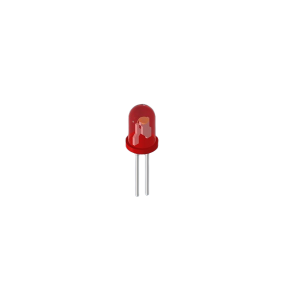
The 940 nm LED, also known as an infrared LED, emits light at a wavelength of 940 nanometers. Unlike visible light, which is in the range of 400 to 700 nanometers, infrared light is not visible to the human eye. This makes 940 nm LED ideal for applications where invisible light is required, such as remote controls, optical communication, and medical imaging.
Characteristics of 940 nm LED
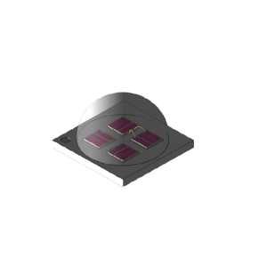
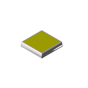
The primary characteristics of 940 nm LED include its low cost, high efficiency, and low power consumption. These LEDs are typically made using gallium arsenide (GaAs) or aluminum gallium arsenide (AlGaAs) as the semiconductor material. The following are some key features of 940 nm LED:
– Low Cost: The manufacturing process for 940 nm LED is relatively simple, which contributes to its low cost. This makes it an attractive option for various applications, especially in the consumer electronics market.
– High Efficiency: These LEDs can convert a significant portion of electrical energy into light, resulting in high efficiency. This is particularly important for battery-powered devices, as it helps to extend their operating time.
– Low Power Consumption: Due to their high efficiency, 940 nm LED consumes less power, which is crucial for energy-saving and environmental protection.
– Long Lifespan: The lifespan of 940 nm LED is typically longer than that of other types of LEDs, making them a reliable choice for long-term applications.
Manufacturing Process of 940 nm LED
The manufacturing process of 940 nm LED involves several steps, including wafer growth, epitaxial layer deposition, device fabrication, and packaging. Here is a brief overview of the process:
– Wafer Growth: The first step is to grow a high-quality gallium arsenide or aluminum gallium arsenide wafer using the molecular beam epitaxy (MBE) technique.
– Epitaxial Layer Deposition: After the wafer is grown, epitaxial layers are deposited onto the wafer to form the LED structure. This process involves the controlled deposition of different semiconductor materials to create the desired optical and electrical properties.
– Device Fabrication: The epitaxial wafer is then processed to create the LED device. This includes etching, doping, and photolithography to form the necessary electrical contacts and p-n junctions.
– Packaging: Finally, the LED device is packaged using a variety of techniques, such as flip-chip bonding, wire bonding, or die attach, to protect it and ensure efficient heat dissipation.
Applications of 940 nm LED
The applications of 940 nm LED are diverse and growing. Some of the most common uses include:
– Remote Controls: 940 nm LED is widely used in remote controls for consumer electronics, such as televisions, air conditioners, and projectors.
– Optical Communication: These LEDs are used in optical communication systems for transmitting data over fiber optic cables at high speeds.
– Medical Imaging: 940 nm LED is employed in medical imaging devices for non-invasive diagnostics and treatment.
– Security Systems: The invisible light emitted by 940 nm LED is used in security systems for covert surveillance and detection.
– Automotive Industry: These LEDs are used in automotive applications, such as reverse lights, brake lights, and indicator lights.
Future Prospects of 940 nm LED
The future of 940 nm LED looks promising, with ongoing research and development aimed at improving its performance and expanding its applications. Some of the key areas of focus include:
– Enhanced Efficiency: Researchers are working on developing new materials and manufacturing techniques to increase the efficiency of 940 nm LED.
– Miniaturization: There is a growing demand for smaller and more compact 940 nm LED devices, which can be integrated into various portable and wearable devices.
– Customization: Tailoring the properties of 940 nm LED to meet specific application requirements is another area of interest.
– Cost Reduction: Efforts are being made to reduce the cost of manufacturing 940 nm LED, making it more accessible for a wider range of applications.
In conclusion, the 940 nm LED has become an essential component in the optoelectronics industry, offering numerous advantages and applications. As technology continues to advance, the potential for 940 nm LED to revolutionize various fields is immense.
Explore More from Queendom Lamp
Stay updated with the latest LED technology, lighting solutions, and industry insights.
Request a Quote About Queendom