


Infrared lamp bead 850nm has become an indispensable component in various industries, providing a unique advantage in terms of heat generation and radiation. This article aims to introduce the industry of infrared lamp beads, focusing on the 850nm wavelength. With a comprehensive overview, we will explore the applications, production process, market trends, and future prospects of this cutting-edge technology.
Introduction to Infrared Lamp Bead 850nm
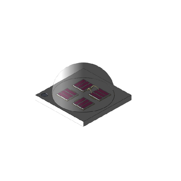
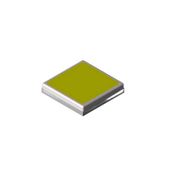
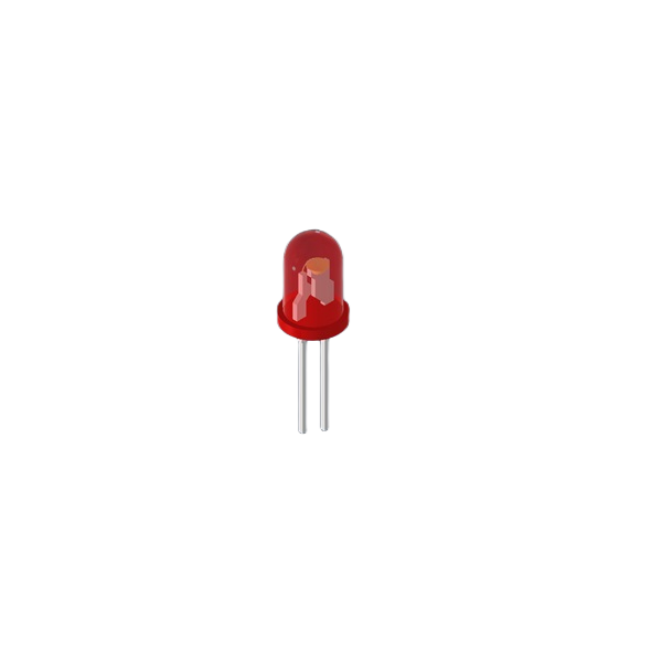
Infrared lamp beads, also known as infrared LEDs, are semiconductor devices that emit infrared light with a specific wavelength. The 850nm wavelength is widely used in various applications due to its unique properties. Compared with other wavelengths, 850nm infrared light has a lower power consumption, higher energy efficiency, and stronger penetration ability. It is widely used in infrared sensors, infrared communication, and infrared heating fields.
Applications of Infrared Lamp Bead 850nm
Infrared lamp beads 850nm have a wide range of applications, including:
- Infrared Sensors: 850nm infrared light is commonly used in infrared sensors for distance measurement, motion detection, and obstacle avoidance. The low power consumption and high sensitivity of this wavelength make it an ideal choice for various applications in the Internet of Things (IoT) field.
- Infrared Communication: 850nm infrared light is used in infrared communication systems, such as remote controls, wireless transmission, and infrared data transmission. It offers a high data transmission rate and strong anti-interference ability.
- Infrared Heating: 850nm infrared light is widely used in infrared heating equipment, such as infrared saunas, infrared cookers, and infrared heating panels. It provides a healthy and energy-saving heating method.
- Medical Equipment: 850nm infrared light is applied in medical equipment for physical therapy, wound healing, and pain relief. It has a significant effect on promoting blood circulation and enhancing the body’s immune function.
Production Process of Infrared Lamp Bead 850nm
The production process of infrared lamp beads 850nm mainly includes the following steps:
- Material Preparation: The raw materials used in the production of infrared lamp beads 850nm mainly include gallium arsenide (GaAs), gallium phosphide (GaP), and other III-V group compound semiconductors.
- Epitaxial Growth: The epitaxial growth process is used to grow the active layer on the substrate. This process involves the epitaxial deposition of the III-V group compound semiconductor material on the substrate, forming a crystal structure with a high degree of order.
- Photolithography and Etching: Photolithography and etching are used to form the light-emitting region and the contact area of the infrared lamp bead. This process involves the exposure of the photoresist and the etching of the substrate to achieve the desired structure.
- Ion Implantation: Ion implantation is used to introduce impurities into the crystal lattice of the semiconductor material, which can improve the optical and electrical properties of the infrared lamp bead.
- Bonding and Packaging: The bonding and packaging process involves the bonding of the infrared lamp bead to the lead frame and the encapsulation of the packaged product. This process ensures the protection and stable performance of the infrared lamp bead.
Market Trends of Infrared Lamp Bead 850nm
The market of infrared lamp beads 850nm is growing rapidly due to the continuous expansion of its applications. The following are some key market trends:
- Increased Demand in IoT Industry: With the rapid development of the Internet of Things, the demand for infrared sensors and other related products is increasing, which drives the growth of the infrared lamp bead market.
- Market Expansion in Infrared Communication: The application of infrared communication technology in various fields, such as home appliances, medical equipment, and industrial automation, promotes the expansion of the infrared lamp bead market.
- Government Support and Policies: Many countries have introduced favorable policies and subsidies to support the development of the semiconductor industry, which in turn benefits the infrared lamp bead market.
- Technological Innovation: Continuous technological innovation in the field of infrared lamp beads 850nm has led to the emergence of new products and applications, further promoting the growth of the market.
Future Prospects of Infrared Lamp Bead 850nm
The future prospects of infrared lamp beads 850nm are promising. With the continuous development of technology and the expansion of applications, the following trends are expected:
- High-Efficiency and Energy-Saving Products: As energy-saving and environmental protection become increasingly important, the development of high-efficiency and energy-saving infrared lamp beads will be a major trend.
- Miniaturization and Integration: The miniaturization and integration of infrared lamp beads will further expand their application fields, such as wearable devices, smart homes, and automotive electronics.
- Customization and Application Innovation: With the deepening of market demand, customized and innovative applications of infrared lamp beads 850nm will emerge, providing more solutions for various industries.
In conclusion, infrared lamp beads 850nm have a wide range of applications and promising future prospects. As technology continues to advance, the market demand for infrared lamp beads will continue to grow, and new applications will be continuously developed. The industry of infrared lamp beads 850nm will play an increasingly important role in various fields and contribute to the development of the global economy.
Explore More from Queendom Lamp
Stay updated with the latest LED technology, lighting solutions, and industry insights.
Request a Quote About Queendom